
Method of manufacturing a semiconductor device

Inactive Publication Date: 2005-09-06
MITSUBISHI ELECTRIC CORP
View PDF7 Cites 0 Cited by
  • Summary
  • Abstract
  • Description
  • Claims
  • Application Information

AI Technical Summary

Benefits of technology

[0017]The present invention was made to resolve the above-discussed problem and has an object of providing a semiconductor device having stability in device characteristics, in which variation in contact resistance between silicon and poly-silicon or between poly-silicon and poly-silicon is reduced. Another object of the invention is to provide a method of manufacturing suitable for the semiconductor device.
[0019]A method of manufacturing a semiconductor device according to the invention comprises the steps of: laminating an insulating oxide film and a first poly-silicon film sequentially in order on a silicon semiconductor layer of first conductivity type; forming an opening by selectively etching the mentioned insulating oxide film and the mentioned first poly-silicon film and exposing a part of the mentioned silicon semiconductor layer of first conductivity type through the mentioned opening; forming an impurity diffused layer of second conductivity type by implanting an impurity of second conductivity type into the exposed portion of the mentioned silicon semiconductor layer of first conductivity type; removing a natural oxidation film from the mentioned impurity diffused layer of second conductivity type and the mentioned first poly-silicon film by applying HF (hydrofluoric acid) treatment; forming a thin uniform oxide film on the surface of the mentioned impurity diffused layer of second conductivity type and on the surface of the mentioned first poly-silicon film from which the natural oxidation film has been removed; forming a second poly-silicon film on the entire surface of the substrate and implanting the impurity of second conductivity type in the mentioned second poly-silicon film; activating the mentioned impurity of second conductivity type implanted in the mentioned second poly-silicon film and diffusing the mentioned impurity of second conductivity type into the mentioned first poly-silicon film through the mentioned thin uniform oxide film; and forming uniformly a removed portion in the mentioned thin uniform oxide film by applying a high temperature annealing treatment for a short time and forming a thin uniform oxide film serving as contact having the uniformly formed removed portion.
[0023]As described above, in the invention, by providing the H2O2 treatment in the cleaning process prior to the formation of the upper layer poly-silicon film, a thin uniform oxide film of about 0.5 nm to 10 nm in thickness (to the extent of permitting the impurity to diffuse through the film) is formed on the surface of the lower layer silicon or poly-silicon film, and after forming the upper layer poly-silicon film, a removed portion is uniformly formed in the thin uniform oxide film by applying the high temperature annealing treatment for a short time using RTP (Rapid Thermal Process). As a result, variation in contact resistance between the upper layer poly-silicon film and the lower layer silicon or poly-silicon film is reduced. Furthermore, by diffusing the impurity into the lower layer poly-silicon film through the thin uniform oxide film in the BiCMOS structure portion, it becomes possible to obtain a semiconductor device having stable device characteristics.

Problems solved by technology

Since the conventional semiconductor device including the direct contact portion between the refractory materials, for example, between silicon and poly-silicon, poly-silicon and poly-silicon or the like, has been manufactured through the foregoing procedure, there arise several problems as discussed below.
As a result, a problem exists in that something abnormal takes place in device characteristics.

Method used


Image

  • Method of manufacturing a semiconductor device
  • Method of manufacturing a semiconductor device
  • Method of manufacturing a semiconductor device

Examples


embodiment 1

[0033]A BiCMOS semiconductor device and a method of manufacturing the same according to the preferred embodiment of the present invention is hereinafter described with reference to the accompanying drawings.

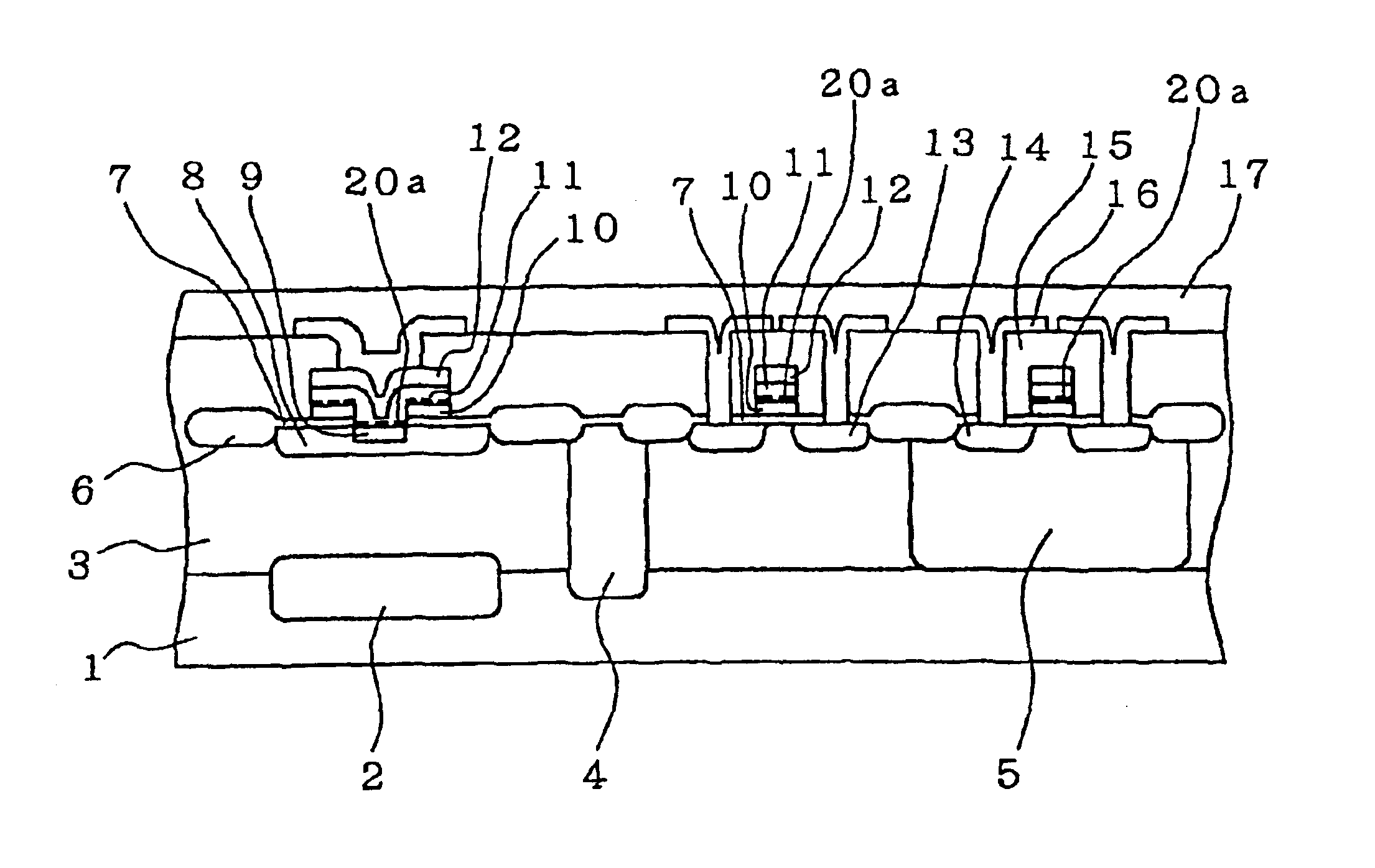
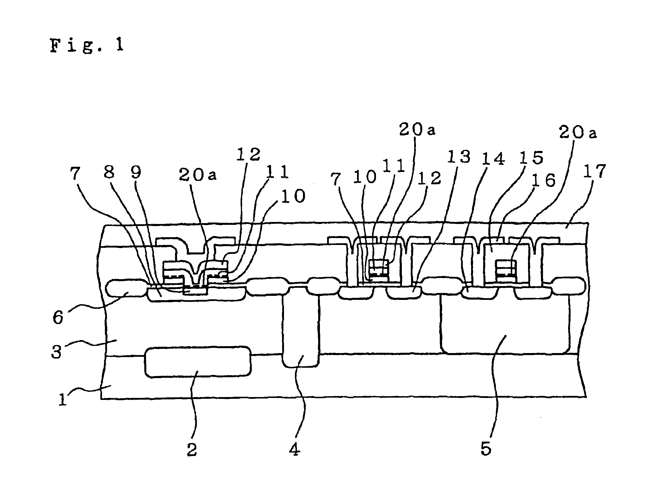
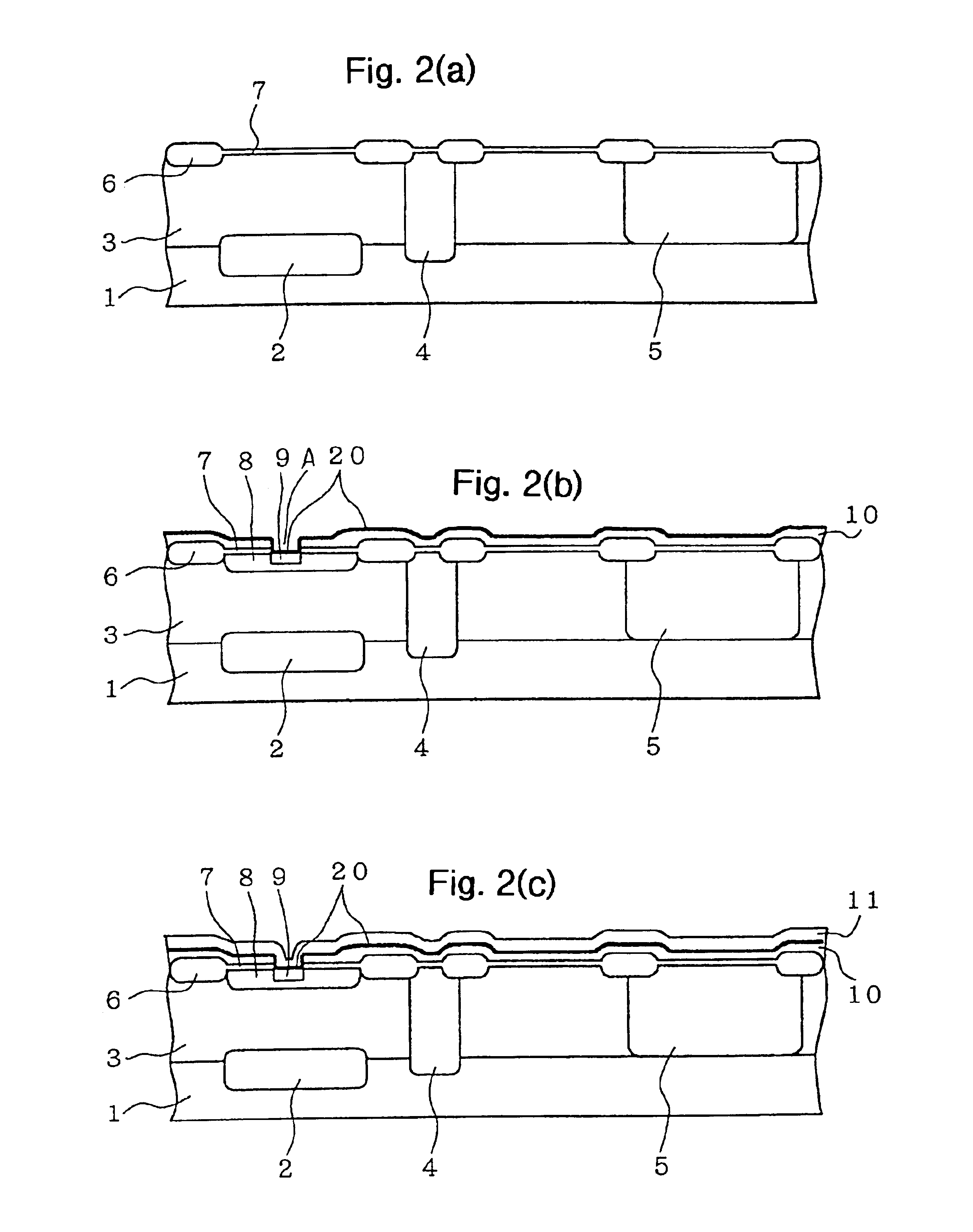
[0034]FIG. 1 is a cross sectional view showing a semiconductor device according to Embodiment 1 of the invention. FIGS. 2(a)-2(c) and 3(a)-3(c) are cross sectional views showing a manufacturing process of the semiconductor device according to Embodiment 1 of the invention.

[0035]In the drawings, reference numeral 1 is a p-type silicon substrate, numeral 2 is an n-type buried duffused layer, numeral 3 is an n-type epitaxial layer, and numeral 4 is a p-type isolation layer. Numeral 5 is a p-type well layer, numeral 6 is a LOCOS (Local Oxidation of Silicon) oxide film, numeral 7 is a gate insulating oxide film, numeral 8 is a p-type base layer, and numeral 9 is an n-type emitter layer. Numeral 10 is a lower layer poly-silicon electrode film, numeral 11 is an upper layer poly-silicon ...


PUM


Abstract

A semiconductor device having stable device characteristics, in which variation in contact resistance between silicon and poly-silicon or between poly-silicon and poly-silicon is reduced. In a cleaning process before forming an upper layer poly-silicon film, a treatment is conducted to form a thin uniform oxide film on the surface of silicon. After forming the upper layer poly-silicon film 11, a removed portion is uniformly formed on the thin uniform oxide film by applying a short time, high temperature annealing treatment.

Description

[0001]This application is a division of U.S. patent application Ser. No. 09 / 966,071, filed on Oct. 1, 2001, abandoned.BACKGROUND OF THE INVENTION[0002]1. Technical Field[0003]The present invention relates to a semiconductor device and to a method of manufacturing the semiconductor device.[0004]2. Background Art[0005]In order to increase a degree of integration and to simplify a manufacturing process in a BiCMOS semiconductor integrated circuit and the like, it has been conventional to employ a method for forming an electrode through direct contact between refractory materials, such as between silicon and poly-silicon or between poly-silicon and poly-silicon.[0006]FIGS. 5, 6 and 7 are drawings to explain an example of BiCMOS semiconductor device according to a prior art that includes a direct contact portion between the refractory materials and a method of manufacturing thereof. In the drawings, reference numeral 1 is a p-type silicon substrate; numeral 2 is an n-type buried and diff...

Claims


Application Information

Patent Timeline
IPC IPC(8): H01L21/70H01L21/8249H01L21/331H01L21/28H01L27/06H01L29/732H01L29/78
CPCH01L21/8249
Inventor IKEGAMI, MASAAKI
Owner MITSUBISHI ELECTRIC CORP
Learn More