Radio frequency switch
a radio frequency switch and frequency technology, applied in electronic switching, pulse technique, semiconductor/solid-state device details, etc., can solve the problems of low power handling efficiency, signal leakage through capacitance, and leakage current degrade isolation, so as to improve power handling and low cost
- Summary
- Abstract
- Description
- Claims
- Application Information
AI Technical Summary
Benefits of technology
Problems solved by technology
Method used
Image
Examples
first embodiment
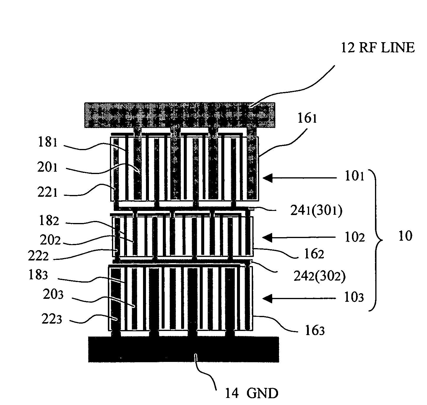
[0027]FIG. 7A is a plan view of an RF switch in accordance with a first embodiment of the present invention. The RF switch in FIG. 7A includes FETs connected in series at three stages. FIG. 7B shows a conventional RF switch having the FETs connected in series at three stages. As will be described below, the width of an electrode interconnection that is connected to a source or drain of the FET at an intermediate (second) stage is narrower than another electrode interconnection that is connected to the source or drain of the FET at an initial (first) stage and an RF line or that is connected to the source or drain of the FET at a final (third) stage and a ground line. The electrode interconnection that is connected to the source of the FET is referred to as a source electrode. The electrode interconnection that is connected to the drain of the FET is referred to as a drain electrode.
[0028]Three FETs 101, 102, and 103 are arranged in three separate FET-forming regions 161, 162, and 16...
second embodiment
[0037]FIG. 9 is a plan view of an RF switch in accordance with a second embodiment of the present invention. Hereinafter, in the second embodiment, the same components and configurations as those of the first embodiment have the same reference numerals. In accordance with the second embodiment of the present invention, the total gate width of the FETs that are arranged in the FET-forming regions 162 at the intermediate (second in the present embodiment) stage(s) is configured to be smaller than the total gate width of the FETs at the initial and final stages. More specifically, each of the FET-forming regions 161 and 163 includes seven FETs. In contrast, the FET-forming region 162 includes six FETs. It is thus possible to reduce the total area of the S / D electrode interconnections 301 and 302, as compared to that in the circuit shown FIG. 7A, and to thereby further reduce the parasitic capacitance Cp to ground. This makes it possible to realize the RF switch having a higher handling...
third embodiment
[0038]FIG. 10 is a plain view of an RF switch in accordance with a third embodiment of the present invention. Hereinafter, in the second embodiment, the same components and configurations as those of the first embodiment have the same reference numerals. The third embodiment has an arrangement in which the FETs arranged in the FET-forming regions 162 at the second (intermediate) stage have a size smaller than that of the FETs at the first and third stage. It is thus possible to further reduce the parasitic capacitance Cp to ground, by shortening the total length of the S / D electrode interconnections 301 and 302. This makes it possible to realize the RF switch having a higher handling power, by lowering the parasitic capacitance Cp to ground without costly additional capacitances and degrading the surge resistance. The third embodiment may be combined with the second embodiment of the present invention.
PUM
 Abstract
Description
Claims
Application Information


