Method for fabricating nonvolatile memory device

a non-volatile memory and fabrication method technology, applied in the direction of semiconductor devices, electrical appliances, basic electric elements, etc., can solve the problems of uniform removal and control of efh, and the conventional asa-sti method may not have the following limitations, so as to improve the uniformity of a threshold voltage and minimize the non-uniformity

Inactive Publication Date: 2009-07-21
SK HYNIX INC
View PDF8 Cites 8 Cited by
  • Summary
  • Abstract
  • Description
  • Claims
  • Application Information

AI Technical Summary

Benefits of technology

[0020]Embodiments of the invention provide a method for fabricating a nonvolatile memory device that can minimize non-uniformity in an effective field oxide height (EFH) in a wafer region, thereby improving the uniformity in a threshold voltage.
[0021]Embodiments of the invention also provide a method for fabricating a nonvolatile memory device that can prevent punch-through events in a dielectric layer caused by a decrease in EFH in a cell region.

Problems solved by technology

However, the conventional ASA-STI method may have the following limitations.
However, this removal is not uniform throughout the wafer (i.e., substrate structure).
Thus, the EFH may not be controlled uniformly throughout the wafer when etching to adjust the EFH.
As described above, because the CMP needs to be performed at least twice according to the ASA-STI method, the resultant structure is prone to the dishing incidence.
The non-uniformity in the EFH within the wafer region may also cause a punch-through event in a dielectric layer interposed between the neighboring floating gates.
The dielectric layer is likely to be damaged in the region where the EFH is low.
If the electric short circuit occurs, leakage current is likely to occur in this region.
The leakage current may impede a stable programming or erasing operation, and this adverse effect may result in device failure, which in turn may decrease device yields.

Method used


Image

  • Method for fabricating nonvolatile memory device
  • Method for fabricating nonvolatile memory device
  • Method for fabricating nonvolatile memory device

Examples


Embodiment Construction

[0031]In the following drawings, the thickness of layers and regions are exaggerated for clarity of the description, and when it is described that one layer is formed on another layer or a substrate, the term “on” indicates that the layer may be formed directly on the other layer or the substrate, or a third layer may be interposed therebetween.

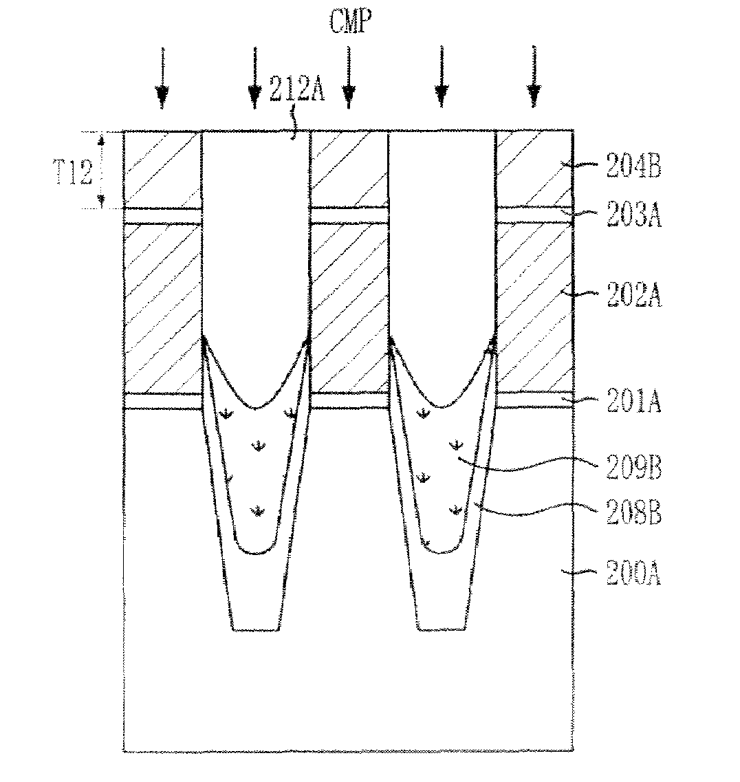
[0032]FIGS. 7A to 7H are cross-sectional views illustrating a method for fabricating a nonvolatile memory device in accordance with an embodiment of the invention. FIGS. 7A to 7H illustrate mainly an isolation structure formed in a cell region for the simplicity of the description, and the detailed description of the isolation structure is provided herein below.

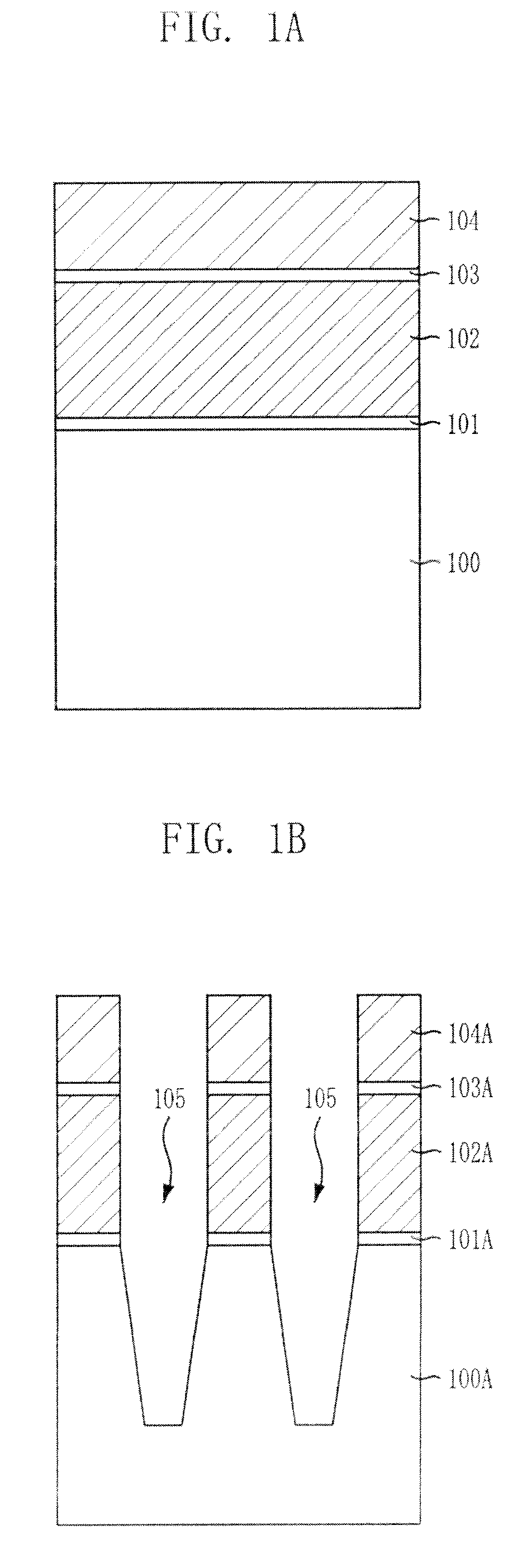
[0033]Referring to FIG. 7A, although not illustrated, a triple N-type well is formed in a P-type substrate 200, and a P-type well is formed inside the triple N-type well. An ion implantation process for adjusting a threshold voltage is performed thereon.

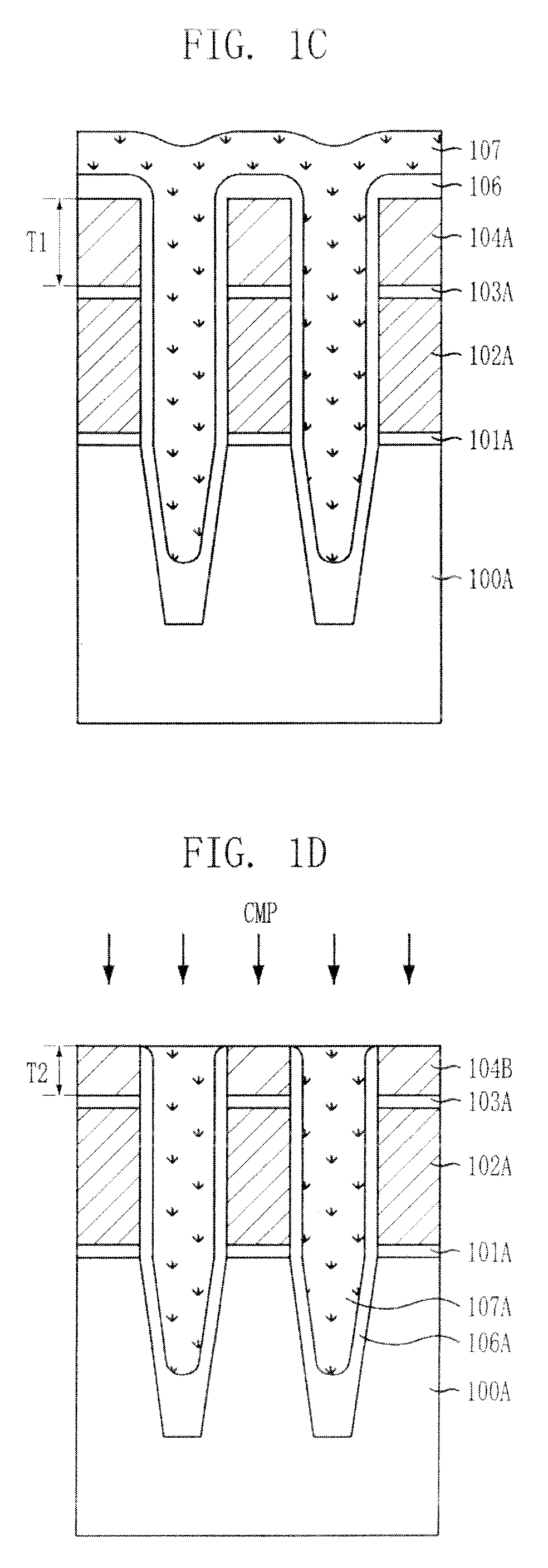
[0034]A gate insulation layer 20...


PUM


Abstract

A method for fabricating a nonvolatile memory device includes forming a gate insulation layer, a first gate conductive layer, a first sacrificial layer, and a second sacrificial layer over a substrate, etching the first and second sacrificial layers, the first gate conductive layer, the gate insulation layer, and the substrate to form trenches, forming a first insulation layer to fill the trenches, polishing the first insulation layer using the etched second sacrificial layer as a polish stop layer, removing the second sacrificial layer, recessing the first insulation layer inside the trenches, forming a second insulation layer to fill a space produced inside the trenches by the recessing of the first insulation layer, and polishing the second insulation layer using the etched first sacrificial layer as a polish stop layer.

Description

CROSS-REFERENCE TO RELATED APPLICATION[0001]The priority of Korean patent application number 10-2007-0032073, filed on Mar. 31, 2007, the disclosure of which is incorporated by reference in its entirety, is claimed.BACKGROUND OF THE INVENTION[0002]The invention relates to a method for fabricating a nonvolatile memory device and, more particularly, to a method for fabricating an NAND flash memory device implemented with an advanced self-aligned shallow trench isolation (ASA-STI) method.[0003]There is a great demand for flash memory devices that can electronically program and erase data without periodically refreshing data. In an attempt to develop a large capacity memory device that can store a large amount of data, many researchers are particularly focusing on improving the level of integration of semiconductor memory devices.[0004]NAND flash memory devices are suggested as one approach to achieve a higher level of integration in the semiconductor memory devices. In general, an NAND...

Claims


Application Information

Patent Timeline
Patent Type & Authority Patents(United States)
IPC IPC(8): H01L21/76
CPCH01L21/76232H01L27/11521H01L27/115H10B69/00H10B41/30H01L21/3213
Inventor HONG, DONG-GYUN
Owner SK HYNIX INC
Why Eureka
Try Eureka