Method for fabricating semiconductor device

a technology of semiconductor devices and exposure equipment, applied in the direction of semiconductor devices, basic electric elements, electrical appliances, etc., can solve the problems of existing technology not being able to achieve, the line width of the exposure equipment used to fabricate the semiconductor device cannot be less than 60 nm, and the profile of the photoresist pattern is also poor, so as to achieve the effect of minimizing non-uniformity

Active Publication Date: 2011-04-12
SK HYNIX INC
View PDF22 Cites 0 Cited by
  • Summary
  • Abstract
  • Description
  • Claims
  • Application Information

AI Technical Summary

Benefits of technology

[0008]Embodiments of the present invention are directed to provide a method for fabricating a semiconductor device, which can minimize non-uniformity occurring during a chemical mechanical polishing (CMP) process in a fine pattern formation process using spacers.

Problems solved by technology

Existing exposure equipment used to fabricate a semiconductor device cannot form a pattern with a line width of less than 60 nm because of its limitation.
However, the existing technology cannot achieve it.
After a secondary exposure process, a photoresist pattern profile is also poor.
However, the typical method for forming the fine patterns of the semiconductor device may have the following limitation.
That is, because the CMP process is performed on the homogeneous oxide layers such as the first and second oxide layers 12 and 14, the control of the polishing process may become difficult so that uniform layers cannot be formed.

Method used


Image

  • Method for fabricating semiconductor device
  • Method for fabricating semiconductor device
  • Method for fabricating semiconductor device

Examples


Embodiment Construction

[0017]FIGS. 3A to 3F illustrate cross-sectional views showing a method for fabricating a semiconductor device in accordance with an embodiment of the present invention.

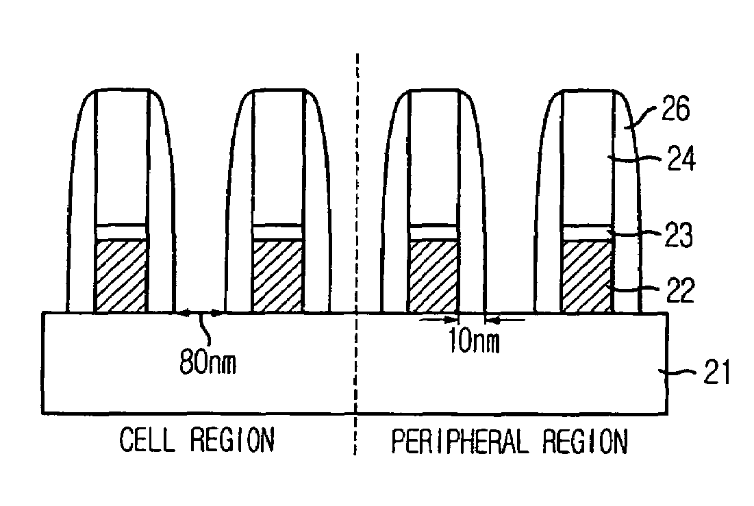
[0018]Referring to FIG. 3A, a semiconductor substrate (not shown) defining a cell region and a peripheral region is prepared. An etch target layer 21 is formed over the semiconductor substrate. A plurality of etch mask patterns including a first hard mask layer 22, a first pad layer 23, and a second pad layer 24 are formed over the etch target layer 21. The first hard mask layer 22, the first pad layer 23, and the second pad layer 24 include polysilicon, a nitride-based material, and an oxide-based material, respectively. Thus, the first hard mask layer 22, the first pad layer 23, and the second pad layer 24 are referred to as the polysilicon layer 22, the nitride layer 23, and the first oxide layer 24 hereinafter. The polysilicon layer 22 is formed of doped polysilicon with phosphorus concentration of approximately 5...


PUM


Abstract

A method for fabricating a semiconductor device includes forming a plurality of etch mask patterns over an etch target layer, each of the etch mask patterns including a first hard mask, a first pad layer, and a second pad layer, forming spacers on both sidewalls of the etch mask patterns, the spacers including a material substantially the same as that of the first pad layer, forming a second hard mask over the resulting substrate structure until gaps between the etch mask patterns are filled, the second hard mask including a material different from that of the first hard mask but substantially the same as that of the second pad layer, planarizing the second hard mask until the first pad layer is exposed, removing the first pad layer and the spacers, and etching the etch target layer using the remaining first and second hard masks as an etch barrier layer.

Description

CROSS-REFERENCE TO RELATED APPLICATIONS[0001]The present invention claims priority of Korean patent application number 10-2006-0018731, filed on Feb. 27, 2006, which is incorporated by reference in its entirety.BACKGROUND OF THE INVENTION[0002]The present invention relates to a semiconductor fabrication technology, and more particularly, to a method for forming fine patterns of a semiconductor device with a line width of less than 50 nm.[0003]Existing exposure equipment used to fabricate a semiconductor device cannot form a pattern with a line width of less than 60 nm because of its limitation. Meanwhile, a double exposure technique is used to form a pattern with a line width of less than 60 nm. In the double exposure technique, however, a develop inspection critical dimension variation occurs during a secondary exposure process according to overlay values. When assuming that a develop inspection critical dimension variation specification is less than ±5 nm in a 50-nm technology, an...

Claims


Application Information

Patent Timeline
Patent Type & Authority Patents(United States)
IPC IPC(8): H01L21/311H01L21/302H01L21/461
CPCH01L21/0337H01L21/0338H01L21/3086H01L21/3088H01L21/31053H01L27/1052H01L21/31116H01L21/32134H01L21/32137H01L27/105H01L21/31111H10B99/00H01L21/304
Inventor KIMPARK, SANG-WOOK
Owner SK HYNIX INC
Why Eureka
Try Eureka