Crack trapping and arrest in thin film structures

a thin film, crack-catching technology, applied in the direction of electrical equipment, semiconductor devices, semiconductor/solid-state device details, etc., can solve the problems of high stress, cracks to originate at chip edges, and thin films are highly susceptible to cracking, etc., to achieve easy addition, reduce the effect of crack energy and cost-effective

Inactive Publication Date: 2009-08-11
GLOBALFOUNDRIES INC
View PDF32 Cites 5 Cited by
  • Summary
  • Abstract
  • Description
  • Claims
  • Application Information

AI Technical Summary

Benefits of technology

[0014]It is an advantage of the present invention that the method of manufacturing the metal plates, having a via-bar structure positioned between the two metal plates, is relatively simple and cost effective. The metal structures comprising the crack trapping structures of the present invention are readily added during conventional BEOL processing. It is a further advantage of the present invention that the design of the crack stop structure of the present invention distributes crack energy more efficiently around a greater area, thereby reducing crack propagation into the chip active area. Cracks are not able to be deflected into a substrate of lower toughness and continue propagating. This is because the cracks are substantially completely trapped between the two metal plates of the crack trapping structure. The stress of the advancing crack is substantially confined to the tough metal area of the via-bar structure.

Problems solved by technology

Such thin films are highly susceptible to cracking during operations such as processing or packaging.
Chip dicing of processed wafers can cause cracks to originate at chip edges.
Packaging can induce high stresses due to thermal expansion mismatch of chip material and packaging material.
The high stresses lead to generation of cracks.
If these cracks reach the active area of the chip, they cause electrical failure of the chip.
Cracks are not able to be deflected into a substrate of lower toughness and continue propagating.
This is because the cracks are substantially completely trapped between the two metal plates of the crack trapping structure.

Method used


Image

  • Crack trapping and arrest in thin film structures
  • Crack trapping and arrest in thin film structures
  • Crack trapping and arrest in thin film structures

Examples


Embodiment Construction

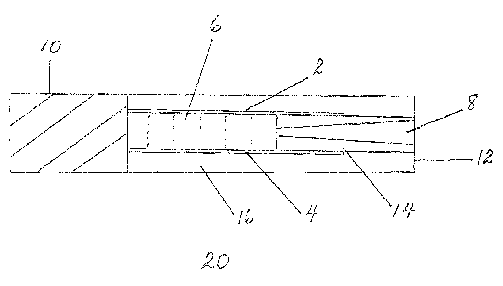
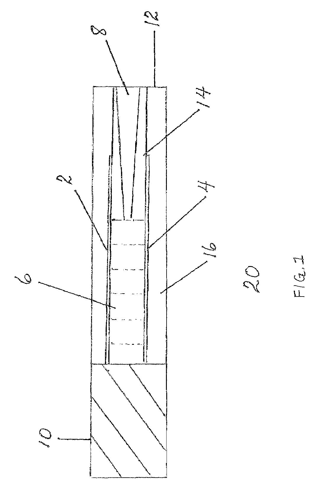
[0019]An embodiment of the present invention is a crack trapping structure that includes two metal plates positioned at the periphery of an IC chip. The two metal plates are connected by a via-bar structure. The via-bar structure is offset from the ends of the metal plates, nearest the edge of the IC chip. Preferably the distance the offset of the via-bar structure is greater than the distance between the two metal plates.

[0020]As shown in FIG. 1, the simplest design of the crack trapping structure of the present invention comprises two metal plates, 2 and 4, positioned around the periphery of an IC chip 20. The chip 20 contains an active area 10. The active area 10 comprises circuitry, diodes, resistors and the like. The two metal plates, 2 and 4, are connected by a via-bar structure 6. The via-bar structure 6 comprises a patterned design of metal walls and vias (holes). The crack trapping structure is easily manufactured; and readily incorporated into the IC chip during the standa...


PUM

PropertyMeasurementUnit
perimeteraaaaaaaaaa
distanceaaaaaaaaaa
areaaaaaaaaaaa

Abstract

The present invention relates to a process for preparing a robust crack-absorbing integrated circuit chip comprising a crack trapping structure containing two metal plates and a via-bar structure sandwiched between said plates.

Description

[0001]The present application is a continuation application based on U.S. patent application Ser. No. 12 / 060,937, filed on Apr. 2, 2008.[0002]The present invention relates generally to the manufacturing process of integrated circuit chips. More specifically, the present invention relates to a crack stop structure to prevent the propagation of cracks during the dicing of wafers into individual chips.BACKGROUND OF THE INVENTION[0003]In order to minimize processing errors, maximize throughput by reducing the amount of time it takes to manufacture a given number of integrated circuit (IC) chips, and ease of handling considerations, a large number of IC chips are processed simultaneously on the surface of a wafer before the wafer is cut or “diced” into the individual chips. However, the dicing process may cause cracks in the active (wired) areas of the IC chips, thus resulting in chip failure. To reduce the amount of chip failure due to crack propagation during dicing and the resultant d...

Claims


Application Information

Patent Timeline
Patent Type & Authority Patents(United States)
IPC IPC(8): H01L23/44
CPCH01L23/562H01L23/585H01L2924/0002H01L2924/00
Inventor SHAW, THOMAS MLANE, MICHAEL WLIU, XIO HUBONILLA, GRISELDADOYLE, JAMES PLANDIS, HOWARD SLINIGER, ERIC G
Owner GLOBALFOUNDRIES INC
Why Eureka
Try Eureka