Methods for integrating lattice-mismatched semiconductor structure on insulators

a technology of semiconductor structure and insulator, applied in the direction of semiconductor devices, basic electric elements, electrical apparatus, etc., can solve the problems of dislocation defects and epitaxial dislocation defects, and achieve the effects of increasing the functionality and performance of the cmos platform, reducing (a) channel resistance, and high mobility

Inactive Publication Date: 2007-03-08
AMBERWAVE SYST
View PDF99 Cites 134 Cited by
  • Summary
  • Abstract
  • Description
  • Claims
  • Application Information

AI Technical Summary

Benefits of technology

[0011] Heterointegration of alternative materials is desirable for various electronic and optoelectronic applications. For example, the heterointegration of III-V, II-VI materials and/or Ge with Si is an attractive path for increasing the functionality and performance of the CMOS platform. An economical solution to heterointegration could enable new fields and applications, such as replacing Si in CMOS transistors, particularly for critical-path logic devices. Heterointegration could significantly lower (a) channel resistance, due to the ultra-high mobility and saturation velocity afforded by various non-Si semiconductors, and (b) source/drain resistance, due both t...

Problems solved by technology

First, it facilitates adding the non-Si semiconductor material only where it is needed, and so is only marginally disruptive to a Si CMOS process performed on the same wafer.
As mentioned above, dislocation defects typically arise during epitaxial growth of one kind of crystal mat...

Method used


Image

  • Methods for integrating lattice-mismatched semiconductor structure on insulators
  • Methods for integrating lattice-mismatched semiconductor structure on insulators
  • Methods for integrating lattice-mismatched semiconductor structure on insulators

Examples


Embodiment Construction

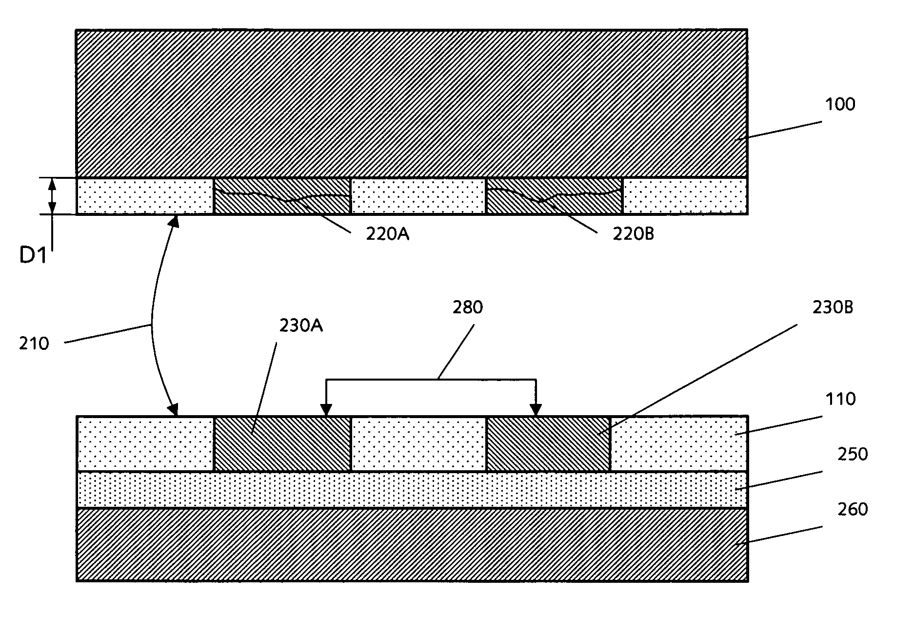
[0025] In accordance with its various embodiments, the invention disclosed herein contemplates fabrication of monolithic lattice-mismatched semiconductor heterostructures disposed over an insulator platform with limited-area regions substantially exhausted of misfit and threading dislocations, as well as fabrication of semiconductor devices based on such lattice-mismatched heterostructures.

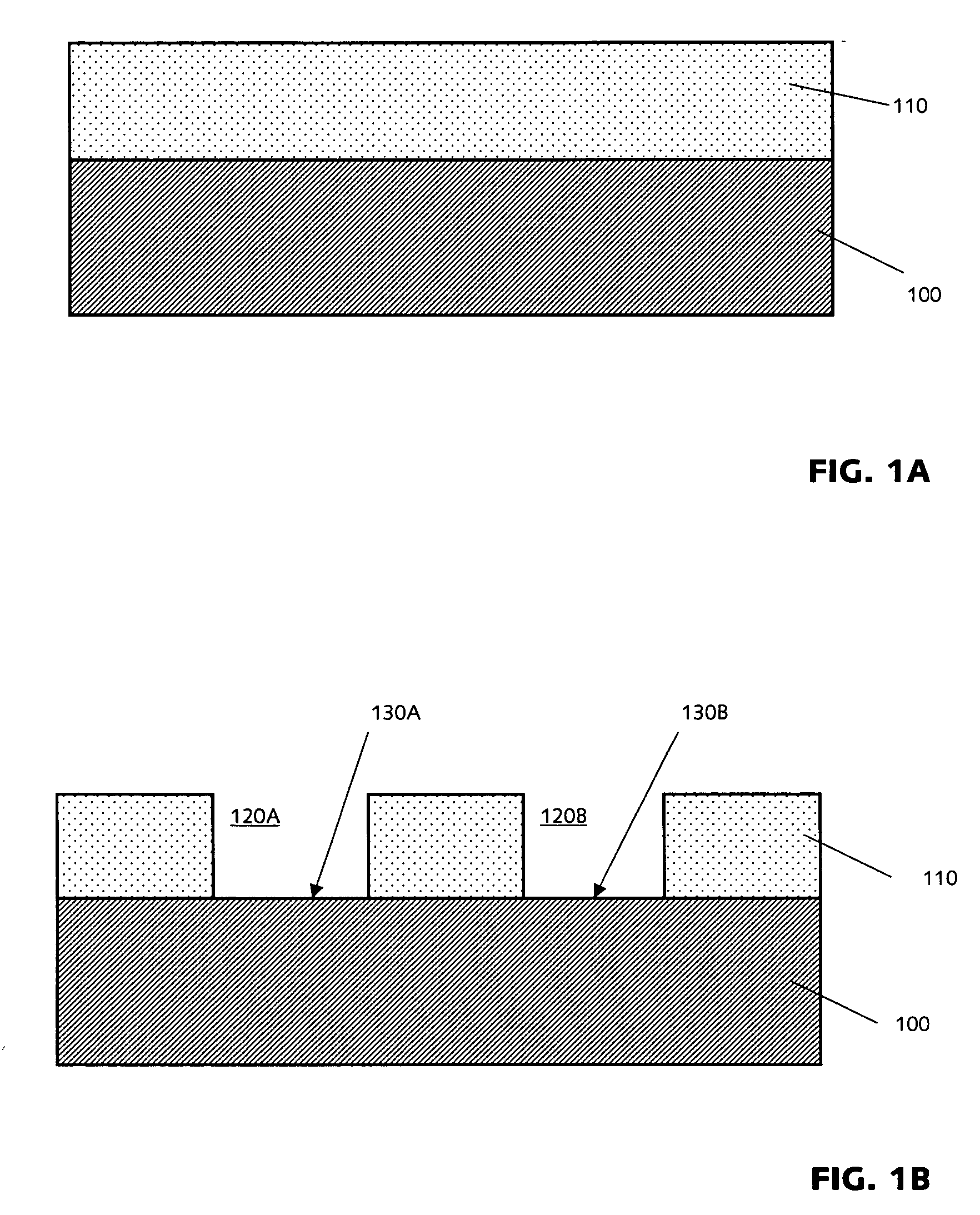
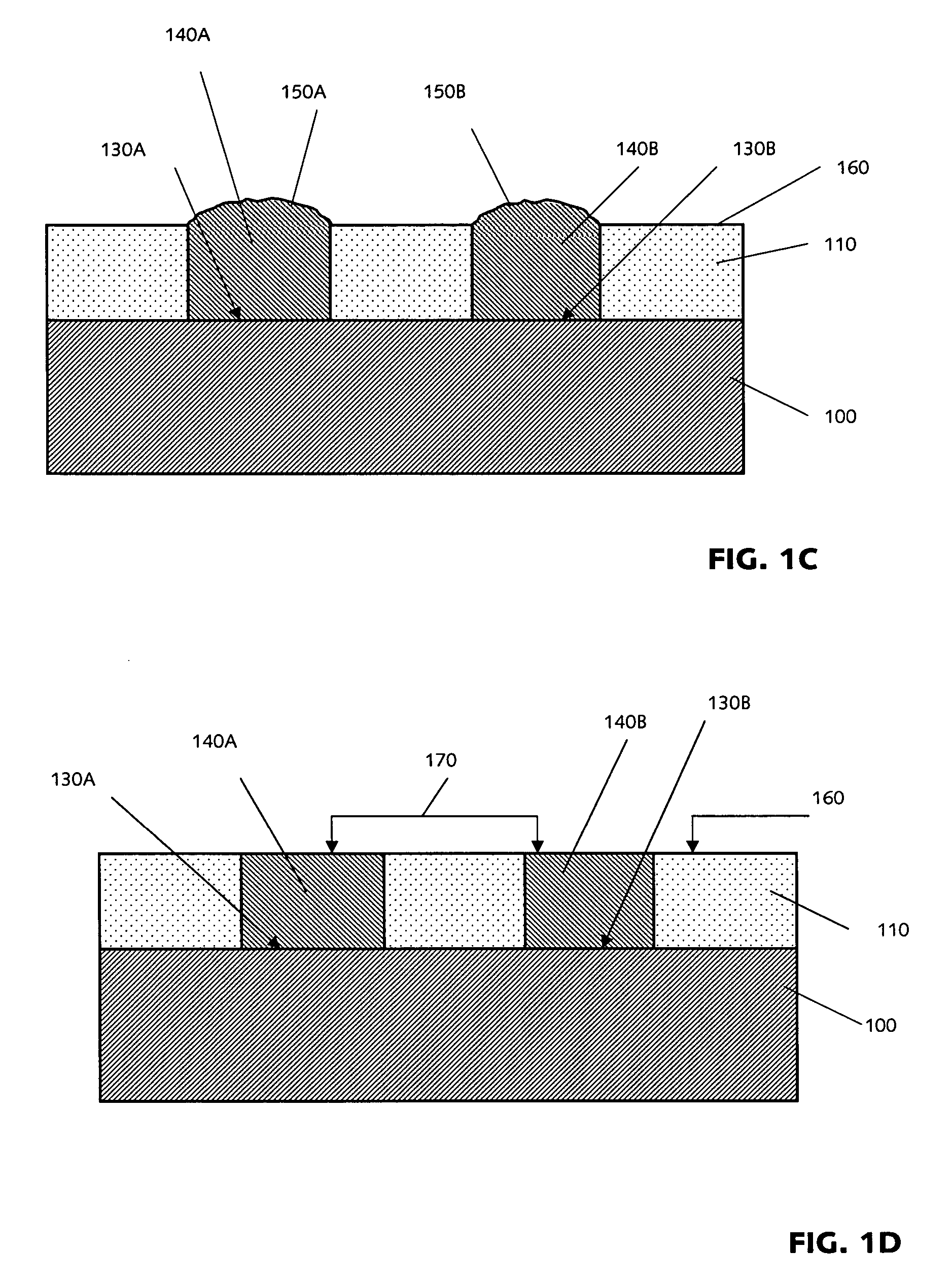
[0026] Referring to FIGS. 1A-1C, planar isolation regions may be utilized for the selective epitaxy of active-area materials. In one embodiment, a substrate 100 includes a crystalline semiconductor material. The substrate may be, for example, a bulk silicon wafer, a bulk germanium wafer, a bulk III-V wafer such as gallium arsenide or indium phosphide, a SOI substrate, or a SSOI substrate. An insulator layer 110 is formed over the substrate, as shown in FIG. 1A. The insulator layer may be, for example, silicon dioxide, aluminum oxide, silicon nitride, silicon carbide, or diamond, and may have a th...


PUM


Abstract

Monolithic lattice-mismatched semiconductor heterostructures are fabricated by bonding patterned substrates with alternative active-area materials formed thereon to a rigid dielectric platform and then removing the highly-defective interface areas along with the underlying substrates to produce alternative active-area regions disposed over the insulator and substantially exhausted of misfit and threading dislocations.

Description

FIELD OF THE INVENTION [0001] This invention relates generally to lattice-mismatched semiconductor heterostructures and, specifically, to methods and materials for formation of integrated structures including alternative active-area materials on insulators. BACKGROUND OF THE INVENTION [0002] The increasing operating speeds and computing power of microelectronic devices have recently given rise to the need for an increase in the complexity and functionality of the semiconductor structures from which these devices are fabricated. Hetero-integration of dissimilar semiconductor materials, for example, III-V materials, such as gallium arsenide, gallium nitride, indium aluminum arsenide, and / or germanium with silicon, siticon-on-insulator, or silicon-germanium substrates, is an attractive path for increasing the functionality and performance of the CMOS platform. Specifically, as geometric scaling of Si-based MOSFET technology becomes more challenging, the heterointegration of alternative...

Claims


Application Information

Patent Timeline
IPC IPC(8): H01L21/30
CPCH01L21/76254H01L21/823807H01L21/823878H01L29/78687H01L27/1203H01L29/7842H01L21/84
Inventor CURRIE, MATTHEWLOCHTEFELD, ANTHONYCHENG, ZHIYUANLANGDO, THOMAS
Owner AMBERWAVE SYST
Why Eureka
Try Eureka