Electric element, memory device, and semiconductor integrated circuit formed using a state-variable material whose resistance value varies according to an applied pulse voltage

a state variable material and semiconductor technology, applied in the direction of digital storage, diodes, instruments, etc., can solve the problems of reducing shortening the read and write time, and complicated production process, so as to increase the resistance value and reduce the resistance value of the layer

Active Publication Date: 2009-08-18
PANASONIC CORP
View PDF9 Cites 56 Cited by
  • Summary
  • Abstract
  • Description
  • Claims
  • Application Information

AI Technical Summary

Benefits of technology

[0019]Since the electric element has the “diode characteristic”, the direction of the electric current can be defined without using a diode element therefor. Further, the electric element has the “variable-resistance characteristic” and therefore can be used as, for example, a 1R1D nonvolatile memory. In such a use, it is not necessary to provide a diode, and therefore, the production process is simplified, as compared with a conventional 1R1D nonvolatile memory. Furthermore, since a diode is not provided, the polarity of a pulse voltage to be applied to the variable-resistance material is not restricted. Therefore, both a pulse voltage of positive (+) polarity and a pulse voltage of negative (−) polarity can be applied to the state-variable material layer. In such a pulse application method (wherein the resistance value is changed according to the polarity of the pulse voltage), the pulse width of a pulse voltage applied is short as compared with a conventional pulse application method (a method wherein the resistance value of the variable-resistance material is changed by adjusting the pulse width of the pulse voltage). That is, the time required for memorization or reset can be shortened.
[0025]In the above electric element, the pulse width of a pulse voltage applied for memorization or reset is short as compared with a conventional pulse voltage. That is, the time required for memorization or reset can be shortened.
[0027]Since the above electric element has the “diode characteristic”, the direction of the electric current can be defined without using a diode element therefor. Thus, the electric element can be used as, for example, a 1R1D nonvolatile memory. In such a use, it is not necessary to provide a diode, and therefore, the production process is simplified, as compared with a conventional 1R1D nonvolatile memory.
[0037]Preferably, the electric element further comprises a voltage driver, the voltage driver applying the pulse voltage between the first electrode and the second electrode such that the first electrode becomes negative with respect to the second electrode to increase the resistance value of the layer for the forward direction; and the voltage driver applying the pulse voltage between the first electrode and the second electrode such that the first electrode becomes positive with respect to the second electrode to decrease the resistance value of the layer for the forward direction.

Problems solved by technology

Further, demands for increasing the capacity of a memory device, reducing the write power, shortening the read and write times, and prolonging the device's life have been escalating.
Such a structure requires a complicated production process and is therefore unsuitable for practical use.
Thus, the polarity of a pulse voltage to be applied to the variable-resistance material is restricted.

Method used


Image

  • Electric element, memory device, and semiconductor integrated circuit formed using a state-variable material whose resistance value varies according to an applied pulse voltage
  • Electric element, memory device, and semiconductor integrated circuit formed using a state-variable material whose resistance value varies according to an applied pulse voltage
  • Electric element, memory device, and semiconductor integrated circuit formed using a state-variable material whose resistance value varies according to an applied pulse voltage

Examples


example 1

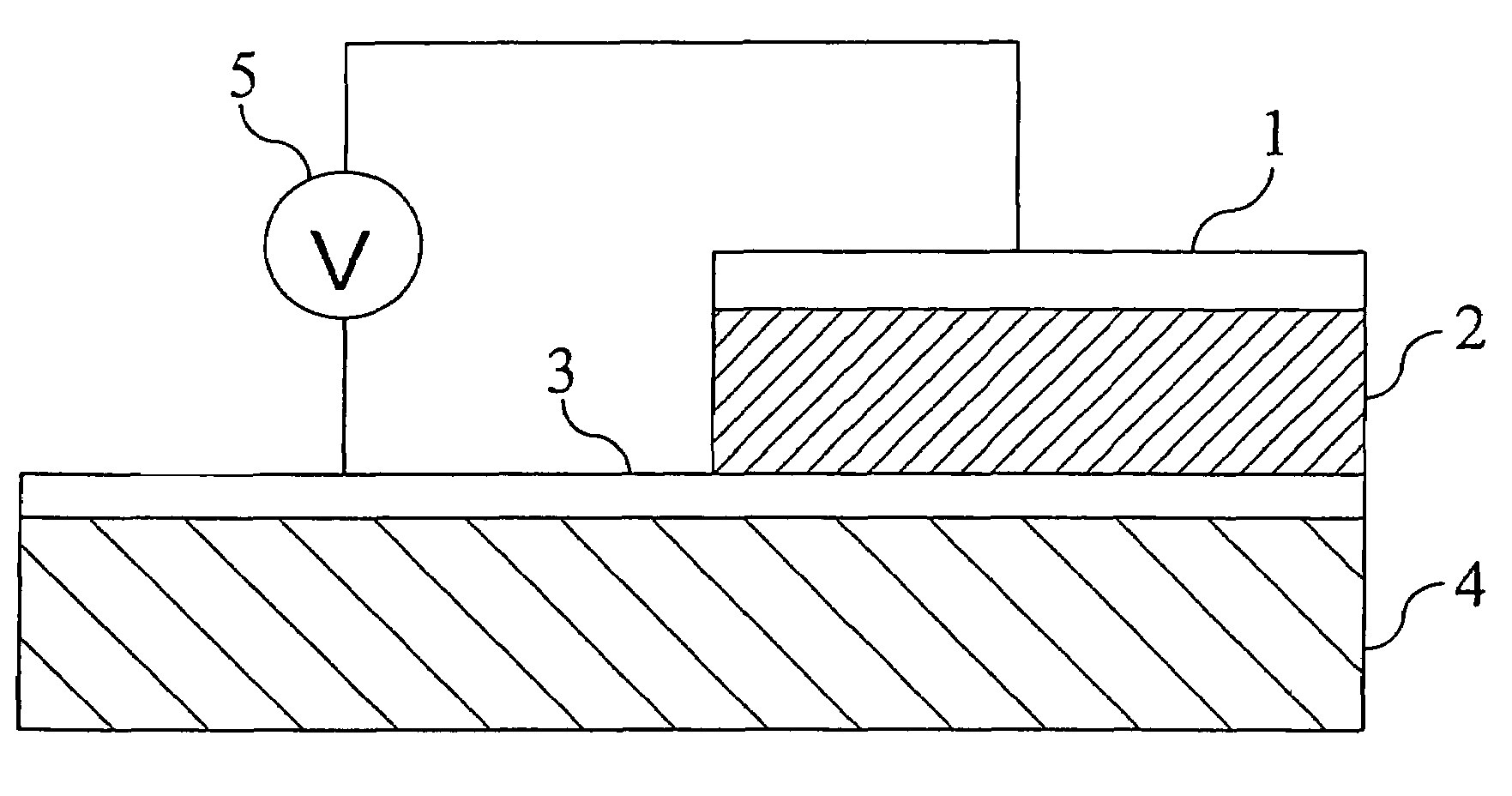
[0069]To realize the state-variable material layer 2 having the above-described characteristics (variable-resistance characteristic and diode characteristic), the upper electrode 1 and the lower electrode 3 are formed of different materials having different work functions in the electric element of FIG. 1. The reasons therefor are described below.

[0070]

[0071]We carried out experiments on the following three types of electric elements.[0072]Sample (A): Electric element in which the work function of the upper electrode 1 is smaller than that of the lower electrode 3.[0073]Sample (B): Electric element in which the work function of the upper electrode 1 is greater than that of the lower electrode 3.[0074]Sample (C): Electric element in which the work function of the upper electrode 1 is equal to that of the lower electrode 3.

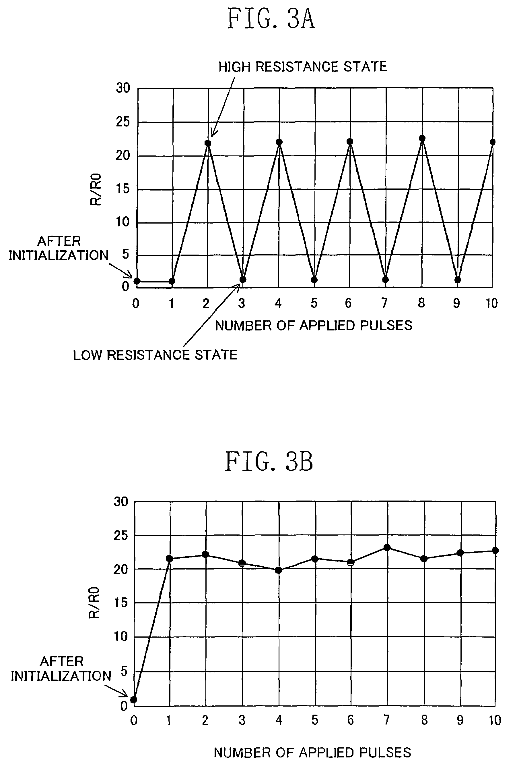
[0075]After the formation of sample (A), sample (B) and sample (C), a pulse voltage (voltage value: +3 V, pulse width: 10 μsec) was applied to the state-variable ma...

example 2

[0176]To realize the state-variable material layer 2 having the above-described characteristics (variable-resistance characteristic and diode characteristic), a state-variable material which has nonuniform crystallinity is used for the state-variable material layer 2 in the electric element of FIG. 1. The reasons therefor are described below.

[0177]

[0178][State-Variable Material Layer Formation Method 1]

[0179]The temperature of the substrate 4 on which the lower electrode 3 has been formed was increased to the vicinity of the crystallization temperature of a state-variable material used for the layer 2 (e.g., about 600° C. for CuFe2O4) to form the state-variable material layer 2. The thus-formed state-variable material layer 2 was subjected to an X-ray diffraction analysis to examine distortion of the crystalline structure, and as a result, it was found that the state-variable material layer 2 exhibits a sharp diffraction peak (a diffraction peak having a large intensity) at a positi...

embodiment 1

[0210]

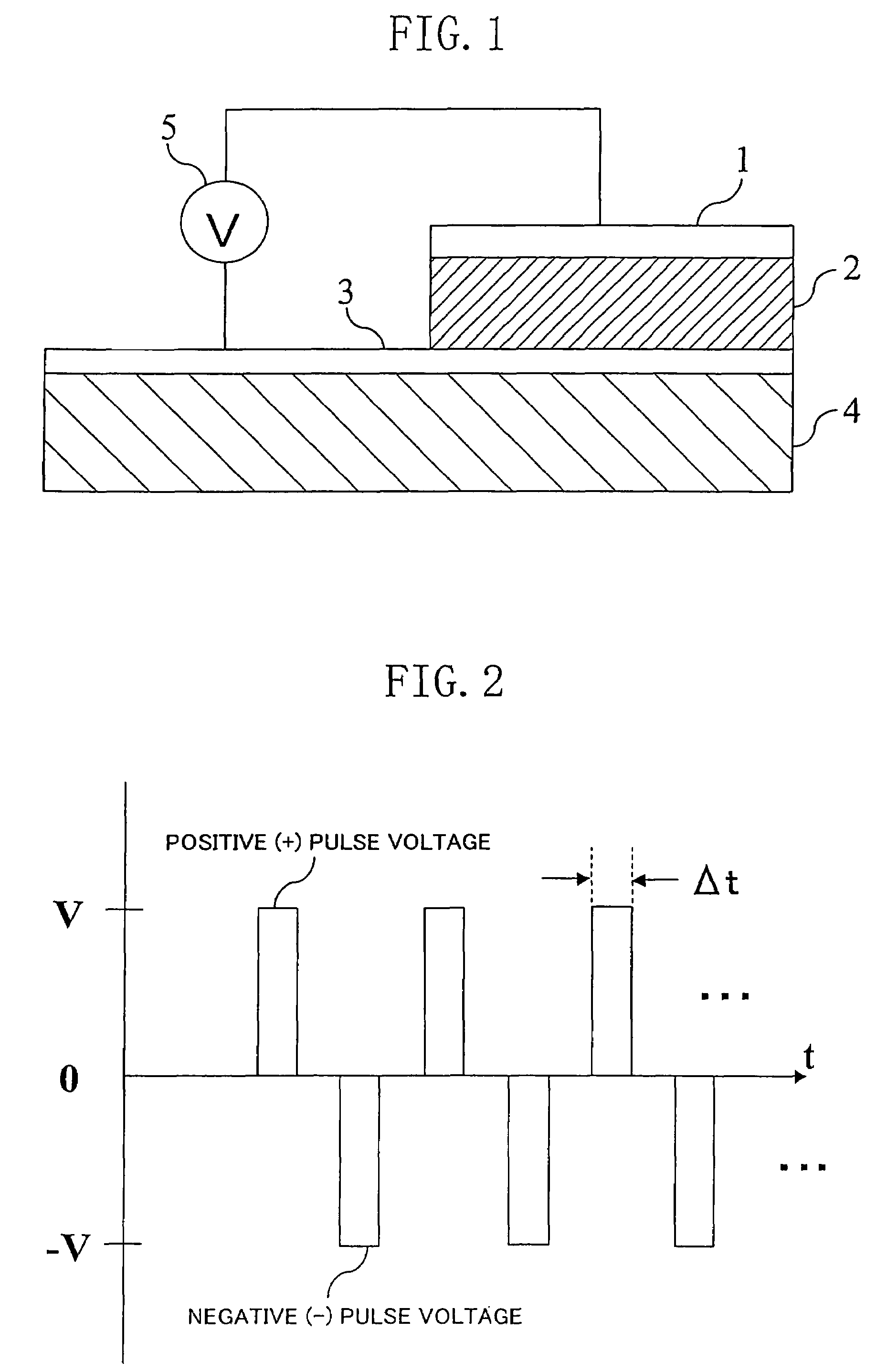
[0211]An electric element of embodiment 1 of the present invention is described. We define the graphical symbol of the electric element of embodiment 1 as shown in FIG. 10. In the electric element 102 shown in FIG. 10, when a pulse voltage is applied between a terminal 101-1 and a terminal 101-2 such that the terminal 101-1 becomes positive (+) with respect to the terminal 101-2, the resistance value of the electric element 102 decreases. When a pulse voltage is applied between the terminal 101-1 and the terminal 101-2 such that the terminal 101-1 becomes negative (−) with respect to the terminal 101-2, the resistance value of the electric element 102 increases. Further, the electric element 102 shown in FIG. 10 exhibits a diode characteristic such that the direction extending from the terminal 101-1 to the terminal 101-2 is “forward direction” and the direction extending from the terminal 101-2 to the terminal 101-1 is “reverse direction”.

[0212]

[0213]Next, the operation of th...


PUM


Abstract

An electric element includes: a first electrode (1); a second electrode (3); and a layer (2) connected between the first electrode and the second electrode and having a diode characteristic and a variable resistance characteristic. The layer (2) conducts a substantial electric current in a forward direction extending from one of the first electrode (1) and the second electrode (3) to the other electrode as compared to a reverse direction opposite of the forward direction. The resistance value of the layer (2) for the forward direction increases or decreases according to a predetermined pulse voltage applied between the first electrode (1) and the second electrode (3).

Description

RELATED APPLICATIONS[0001]This application is the U.S. National Phase under 35 U.S.C. § 371 of International Application No. PCT / JP2005 / 017099, filed on Sep. 9, 2005, which in turn claims the benefit of Japanese Application No. 2005-125686, filed on Apr. 22, 2005, the disclosures of which Applications are incorporated by reference herein.TECHNICAL FIELD[0002]The present invention relates to an electric element, memory device, and semiconductor integrated circuit formed using a state-variable material whose resistance value varies according to an applied pulse voltage.BACKGROUND ART[0003]In recent years, along with the advancement of the digital techniques in electronic devices, demands for nonvolatile memory devices have been increasing for storage of data, such as a picture, and the like. Further, demands for increasing the capacity of a memory device, reducing the write power, shortening the read and write times, and prolonging the device's life have been escalating. To meet such ...

Claims


Application Information

Patent Timeline
Patent Type & Authority Patents(United States)
IPC IPC(8): G11C11/00
CPCG11C11/5685H01L27/2463G11C13/0069H01L27/101H01L27/1021H01L29/8615H01L45/04H01L45/1233H01L45/147G11C13/0007G11C2013/0073G11C2013/0083G11C2213/15G11C2213/31G11C2213/72G11C2213/77H10B63/80H10N70/20H10N70/8836H10N70/826H01L21/02107
Inventor MURAOKA, SHUNSAKUOSANO, KOICHIMITANI, SATORUSEKI, HIROSHI
Owner PANASONIC CORP
Why Eureka
Try Eureka