Unlock instant, AI-driven research and patent intelligence for your innovation.

Shared memory device

a memory device and shared technology, applied in the direction of memory adressing/allocation/relocation, digital storage, instruments, etc., can solve the problems of interconnection, interconnection is induced, interconnection becomes very complex, etc., to achieve the effect of reducing frequency, reducing performance, and increasing area

Inactive Publication Date: 2009-09-08
SONY CORP +1
View PDF15 Cites 21 Cited by
  • Summary
  • Abstract
  • Description
  • Claims
  • Application Information

AI Technical Summary

Benefits of technology

The present invention provides a shared memory device that simplifies interconnects up to memories, prevents a reduction of performance due to increased area and longer interconnects, and increases speed of memory access. The device includes multiple access clusters, each containing a processing module and a memory system with a memory macro and a memory interface. The memory interface faces the processing module and the memory banks are connected in parallel in a second direction, which intersects with the first direction. The input / output port, memory interfaces, and memory banks are connected by interconnects arranged in both directions. This arrangement forms a matrix form in the region of the memory macros. The device also includes a sub processing module for selectively accessing a memory bank. Overall, the device simplifies interconnects, prevents a reduction of performance, and increases speed of memory access.

Problems solved by technology

Further, in the configuration of FIG. 2, the logic circuits 1 can refer to the data of the adjacent logic circuits 1 without going through a higher device, but there are the disadvantages that the interconnects from the logic circuits 1 to the memories 2 become very complex and a reduction of performance (reduction of frequency etc.) due to the increased area and longer interconnect is induced.
Further, as shown in FIG. 3, when a plurality of logic circuits (processors) simultaneously access the same memory, even when the memory macros do not compete, competition of memory interfaces and buses in the memories occurs, therefore simultaneous access is usually not possible.
If increasing the numbers of the memory interfaces and the buses in the memories to enable simultaneous access in order to overcome this, a reduction of performance (reduction of frequency) due to the further increased area and the increase of interconnect length along with this is induced.

Method used


Image

  • Shared memory device
  • Shared memory device
  • Shared memory device

Examples


first embodiment

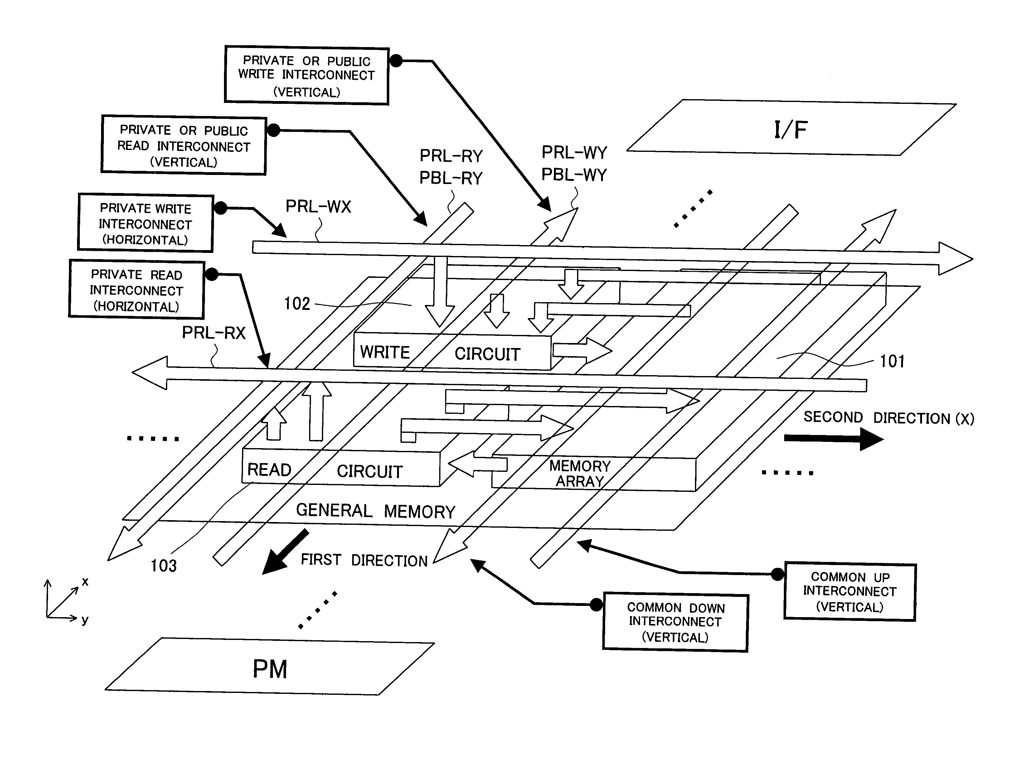
[0083]FIG. 4 is a diagram of the system configuration of a shared memory device according to the present invention.

[0084]A common memory system 10 of FIG. 4 has a plurality of (four in FIG. 4) access clusters 20, 30, 40, and 50 as principal components.

[0085]The access cluster 20 has a processing module (PM0) 21 having one input / output port 211 and a plurality of (two in FIG. 4) memory systems 22 and 23 such as DRAMs or SRAMs which can be accessed by the processing module 21.

[0086]The memory system 22 is provided with a memory macro 221 including a plurality of banks 221-1 to 221-n (n=4 in the present example) arranged in one column in the Y-direction (first direction) of a Rectangular coordinate system set in FIG. 4 and a memory interface (I / F) 222 for interfacing data transfer between the banks 221-1 to 221-n of the memory macro 221 and the processing module 21 and for access control etc. to the banks 221-1 to 221-n. The memory interface 222 is arranged at a position facing the pos...

second embodiment

[0164]FIG. 40 is a diagram of the system configuration of a shared memory device according to the present invention.

[0165]The second embodiment differs from the above first embodiment on the point that at least one side (left side in FIG. 40) of the arrangement region of the memory macros of the access clusters 20 and 40 in the X-direction (second direction) is provided with sub processing module groups 80 and 81 able to selectively access a predetermined at least one memory bank of the plurality of memory macros in the X-direction (second direction).

[0166]The sub processing module group 80 is configured by four sub processing modules 80-1 to 80-4 arranged in accordance with the number of banks of the memory macros of the access clusters 20 and 30. The sub processing module group 81 is configured by four sub processing modules 81-1 to 81-4 arranged in accordance with the number of banks of the memory macros of the access clusters 40 and 50.

[0167]In FIG. 40, among the group of memory...


PUM


Abstract

A shared memory device able to simplify interconnects up to memories, able to prevent a reduction of performance due to an increase of area and longer interconnects, and able to speed up memory access, wherein an input / output port of a processing module, memory interfaces, and memory banks are connected by connection interconnects arranged in a matrix in a first direction and a second direction above an arrangement region of a plurality of memory macros.

Description

CROSS REFERENCE TO RELATED APPLICATION[0001]The present invention contains subject matter related to Japanese Patent Application No. 2005-257074 filed in the Japan Patent Office on Sep. 5, 2005, the entire contents of which being incorporated herein by reference.BACKGROUND OF THE INVENTION[0002]1. Field of Invention[0003]The present invention relates to a shared memory device having a plurality of memory systems including processors or other processing devices mounted thereon and sharing memories of the systems.[0004]2. Description of the Related Art[0005]In a system mounting a plurality of memory systems, when an architecture stressing parallel processing is employed, for example, a configuration as shown in FIG. 1 is exhibited. In the configuration of FIG. 1, since priority is given to parallel processing, logic circuits (processors) 1-1 to 1-4 and memory macros 2-1 to 2-4 are connected in one-to-one correspondence. In the configuration of FIG. 1, while logic circuits 1 and memory...

Claims


Application Information

Patent Timeline
Patent Type & Authority Patents(United States)
IPC IPC(8): G06F13/00
CPCG11C5/025G11C7/1006G11C7/10G06F12/00
Inventor KASHIWAYA, MOTOFUMIYAMAZAKI, TAKESHIHAYASHI, HIROSHI
Owner SONY CORP