

Method of avoiding haze formation on surfaces of silicon-containing PECVD-deposited thin films
a technology of pecvd and thin films, which is applied in the direction of sustainable manufacturing/processing, coatings, and final product manufacturing, can solve the problems of increasing the difficulty of controlling the uniformity of individual films produced across the increased surface area, and the instability of a-si:h gate dielectrics with sinsub>x/sub>, so as to reduce the amount of power and improve the effect of film surface roughness
- Summary
- Abstract
- Description
- Claims
- Application Information
AI Technical Summary
Benefits of technology
Problems solved by technology
Method used
Image

Examples
example one
[0079]FIG. 7 shows a process step diagram 700 which illustrates one embodiment of the invention, where a layer of a silicon-containing material is PECVD deposited using a combination of silicon-containing precursor gas and a non-reactive gas 702; where the flow of the silicon-containing precursor gas is discontinued, and a portion of the non-reactive gas may optionally be discontinued 704; and where the power applied to produce a plasma is either discontinued 706 or ramped down 708. This is an example of a series of steps which is frequently carried out when it is desired to change the film which is being PECVD deposited from a silicon-containing film to a non-silicon containing film; or simply to discontinue PECVD film deposition when the final layer of film being deposited is a silicon-containing film.
example two
[0080]FIG. 8 shows a graph 800 for a set of test conditions used to determine whether the inventors concepts related to a method of preventing a haze during formation of a silicon-containing film were correct. FIG. 8 is provided for comparative purposes, as a contaminant haze was observed on the surface of the silicon nitride film formed under the process conditions illustrated. The FIG. 8 graph 800 illustrates the RF power application, gas flows, and process chamber pressure changes which occur as time progresses. The time shown on time line 801 is in seconds.
[0081]Curve 802 illustrates the amount of RF power applied to maintain the plasma in the processing chamber. At 803 on the curve, the RF power was 18 KW. The power was completely shut down at 804 on curve 802. Curve 812 shows the SiH4 gas flow rate, where the gas flow rate was 5,000 sccm at 813 and decreased to 0 sccm at 814. Curve 822 shows the nitrogen gas flow rate, where the gas flow rate was 55,000 sccm at 823 and decreas...
example three
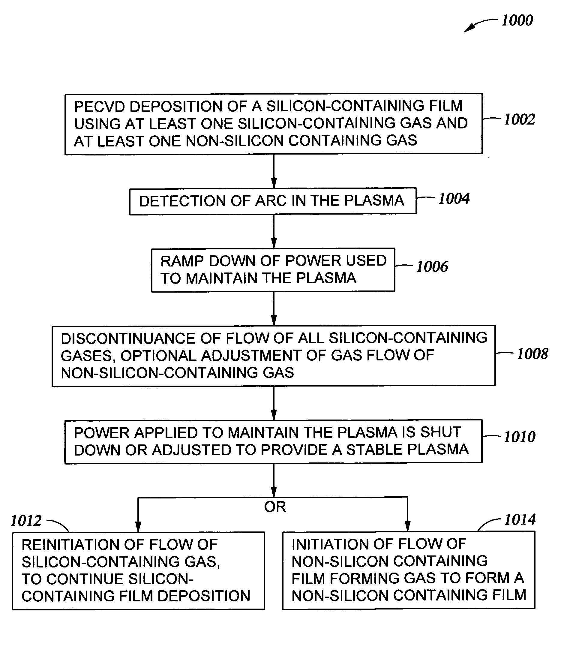
[0085]FIG. 10 shows a process step diagram 1000 which illustrates one embodiment of the invention, where a layer of a silicon-containing material is PECVD deposited using a combination of silicon-containing gas, and at least one non-silicon-containing gas 1002; where an arc in the plasma is detected during film formation 1004, and the power applied to produce the plasma is ramped down, to reduce the potential for damage to the process chamber, but is maintained at a level which continues to support a plasma 1006. The flow of any silicon-containing gas is then discontinued, and a portion of the non-silicon-containing gases which make up the plasma may optionally be increased or decreased 1008. Within a time period typically ranging between about 0.5 and about 3.0 seconds after discontinuance of the silicon-containing gas, the power to the plasma is discontinued 1010. In the alternative, when an arc is detected, at the discretion of the operator of the equipment, an effort may be made...
PUM
| Property | Measurement | Unit |
|---|---|---|
| time | aaaaa | aaaaa |
| time period | aaaaa | aaaaa |
| time | aaaaa | aaaaa |
Abstract
Description
Claims
Application Information