Method and apparatus for programming nonvolatile memory

a nonvolatile memory and programming method technology, applied in the field can solve the problems of unwanted programming of unselected memory cells adjacent to each other, complicated programming operation of nonvolatile memory cells,

Inactive Publication Date: 2009-09-22
MACRONIX INT CO LTD
View PDF20 Cites 4 Cited by
  • Summary
  • Abstract
  • Description
  • Claims
  • Application Information

AI Technical Summary

Benefits of technology

[0011]In some embodiments, the third bit line voltage reduces a magnitude of current from the second bit line through any nonvolatile memory cells on the second bit line side of the nonvolatile memory cell to be programmed. For example, the magnitude of current from the second bit line through any nonvolatile memory cells on the second bit line side of the nonvolatile memory cell is limited to less than one fifth of a magnitude of current through the nonvolatile memory cell to be programmed.
[0012]In some embodiments, the third bit line voltage reduces a magnitude of drain-to-source voltage of any nonvolatile memory cells on the second bit line side of the nonvolatile memory cell to be programmed. For example, the magnitude of drain-to-source voltage of any nonvolatile memory cells on the second bit line side of the nonvolatile memory cell is limited to less than one quarter of a magnitude of drain-to-source voltage of the nonvolatile memory cell.
[0013]In some embodiments, the third bit line voltage substantially prevents programming of any nonvolatile memory cells on the second bit line side of the nonvolatile memory cell.

Problems solved by technology

The program operation of a nonvolatile memory cell is complicated by the program disturb effect.
In the program disturb effect, programming of a selected cell leads to unwanted programming of unselected memory cells adjacent to the selected cell.
In particular, the program disturb effect leads to unwanted programming of memory cells that are: 1) located in columns adjacent to the column including the selected cell and 2) connected to the selected row line (the word line providing a gate voltage to the selected cell).
The integrity of the memory array is adversely affected by these problems For example, the drain-to-source voltage Vds of the disturbed cell can be about 2.5 V, and drain current about 35-45 uA, shifting the threshold voltage more than 50 mV.
Applying a program voltage to not just a bit line adjacent to the memory cell to be programmed, but also to additional bit lines of memory cells that would otherwise be subject to the program disturb effect, does not appear to solve the program disturb effect.

Method used


Image

  • Method and apparatus for programming nonvolatile memory
  • Method and apparatus for programming nonvolatile memory
  • Method and apparatus for programming nonvolatile memory

Examples


Embodiment Construction

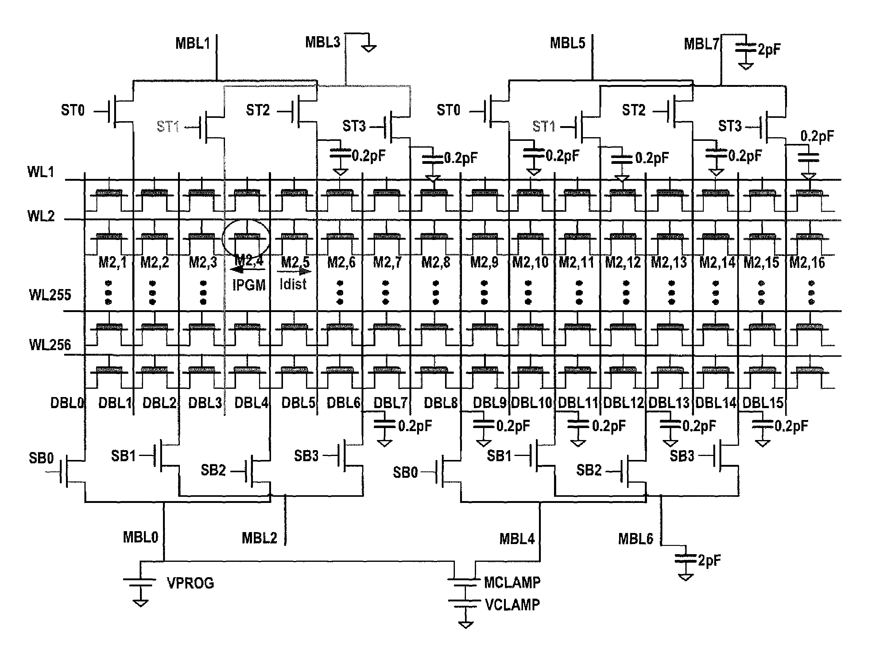
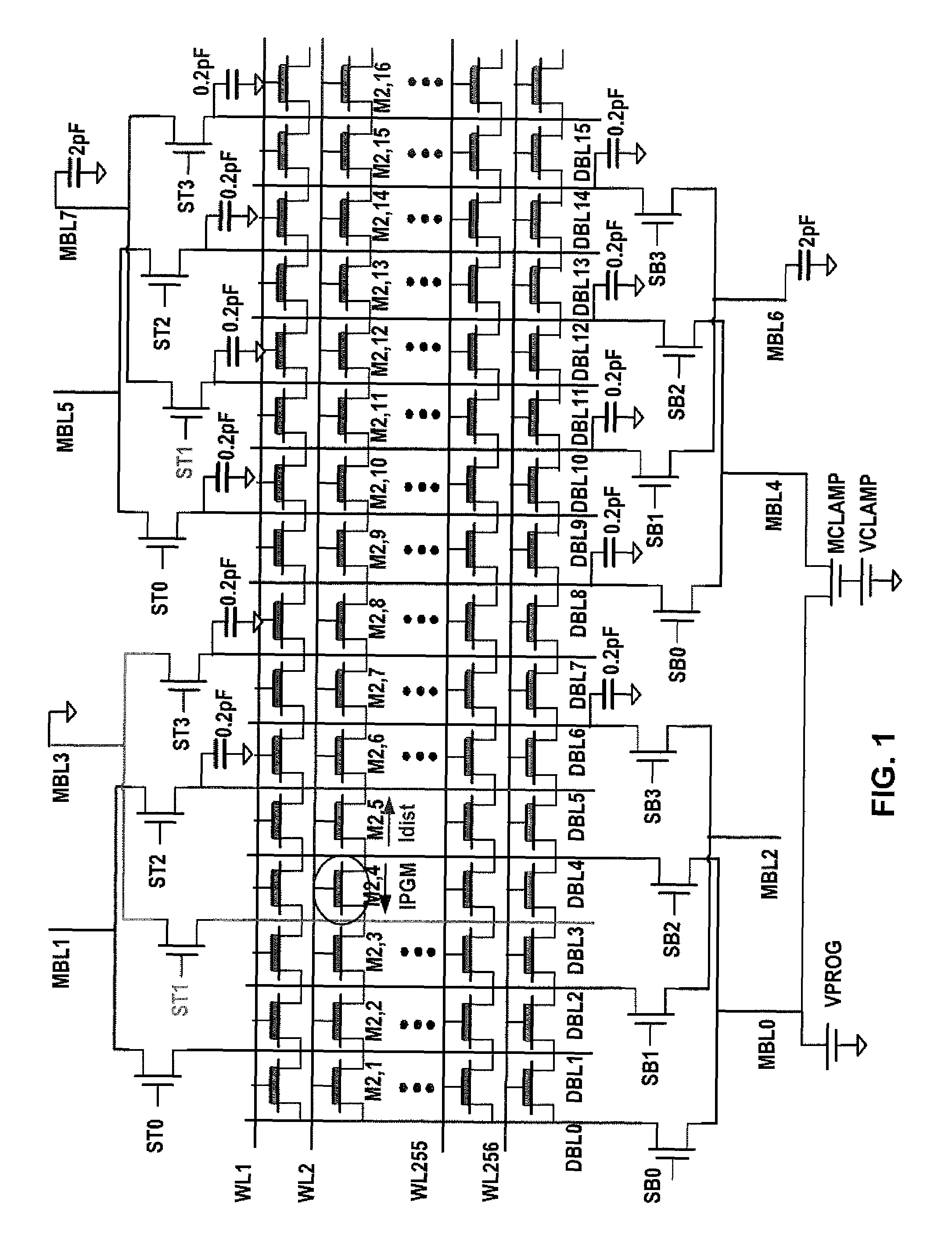
[0028]FIG. 1 shows a nonvolatile memory array accessed by word lines, diffusion bit lines, and metal bit lines, which reduces or eliminates the program disturb effect. The array is arranged in rows and columns. The rows of nonvolatile memory cells are accessed by word lines WL1, WL2, . . . , WL255, and WL256. The columns of nonvolatile memory cells are accessed by diffusion bit lines DBL0, DBL1, . . . , etc. The diffusion bit lines are in turn selectively electrically connected to metal bit lines MBL0, MBL1, . . . , etc.

[0029]A set of select lines and transistors selectively electrically connect each metal bit line to multiple diffusion bit lines, as follows:

[0030]Metal bit line MBL1 is electrically connected to the drain of a transistor whose source is electrically connected to diffusion bit line DBL1, and whose gate is electrically connected to select line ST0. Similarly, metal bit line MBL1 is also electrically connected to the drain of a transistor whose source is electrically c...


PUM


Abstract

Embodiments of addressing the programming disturb effect are shown. A medium voltage having a magnitude between the programming voltage and ground is applied to a metal bit line among the cells that are subject to the program disturb effect.

Description

REFERENCE TO RELATED APPLICATION[0001]This application claims the benefit of U.S. Provisional Patent Application No. 60 / 757,344, filed 9 Jan. 2006 by inventors Yi-Te Shih, Jer-Hau Hsu, Yi-Ti Wang and Hsueh-Yi Lee entitled Method and Circuit Implementation of Preventing Program Disturb.BACKGROUND OF THE INVENTION[0002]1. Field of the Invention[0003]The present technology relates to nonvolatile memory cells, and in particular to nonvolatile memory cells subject to the program disturb effect.[0004]2. Description of Related Art[0005]The program operation of a nonvolatile memory cell is complicated by the program disturb effect. Programming refers to adding charge to, or removing charge from, selected memory cells of a memory array, unlike the indiscriminate erase operation which resets typically an entire sector of memory cells to the same charge storage state. The invention encompasses both products and methods where programming refers to making the net charge stored in the charge trap...

Claims


Application Information

Patent Timeline
Patent Type & Authority Patents(United States)
IPC IPC(8): G11C16/04
CPCG11C16/0491G11C16/3459G11C16/3427G11C16/12
Inventor SHIH, YI TEHSU, JER-HAOWANG, YI-TILEE, HSUEH-YI
Owner MACRONIX INT CO LTD
Why Eureka
Try Eureka