Logic cell array and bus system

a logic cell and bus system technology, applied in the field of logic cell arrays, can solve the problems of large number of cells having to communicate with each other, system becomes problematic, system may not work well, etc., and achieve the effect of optimal chip form and easy linking of data

Active Publication Date: 2009-09-29
SCIENTIA SOL MENTIS AG
View PDF542 Cites 59 Cited by
  • Summary
  • Abstract
  • Description
  • Claims
  • Application Information

AI Technical Summary

Benefits of technology

[0009]According to example embodiments of the present invention, in a logic cell array having a number of logic cells and a segmented bus system for logic cell communication, the bus system includes different segment lines having shorter and longer segments for connecting two points in order to be able to minimize the number of bus elements traversed between separate communication start and end points.
[0010]By configuring the busses using segments of great length that are fashioned as a single line for bypassing long paths in a logic cell array, an especially simple design and an especially efficient operation result. By simultaneously providing short segment lines, it is ensured that all points are addressable as needed.

Problems solved by technology

One of the difficulties with conventional systems is that a large number of cells have to communicate with each other.
Such a system becomes problematic when a great many communicating units need access to the bus or busses.
In systems like logic cell arrays, in which very rapid communication is desired in order to ensure high data processing speeds, this is an undesirable solution.
However, this system may not work well when integrated on semiconductor chips, such as in CMOS technology, where the structure is typically complex and the operation is energy inefficient.
Furthermore, when busses are very long, data processing can be prevented from being properly completed if the long periods of time until the data arrive at the destination when paths are long and (in some cases) the return of the reception confirmation is taken into account.
The hardware technology implementation of these elements then requires substantial space, which may be considerable compared to that of the lines to be disposed in the intermediate layers.

Method used


Image

  • Logic cell array and bus system
  • Logic cell array and bus system
  • Logic cell array and bus system

Examples


Embodiment Construction

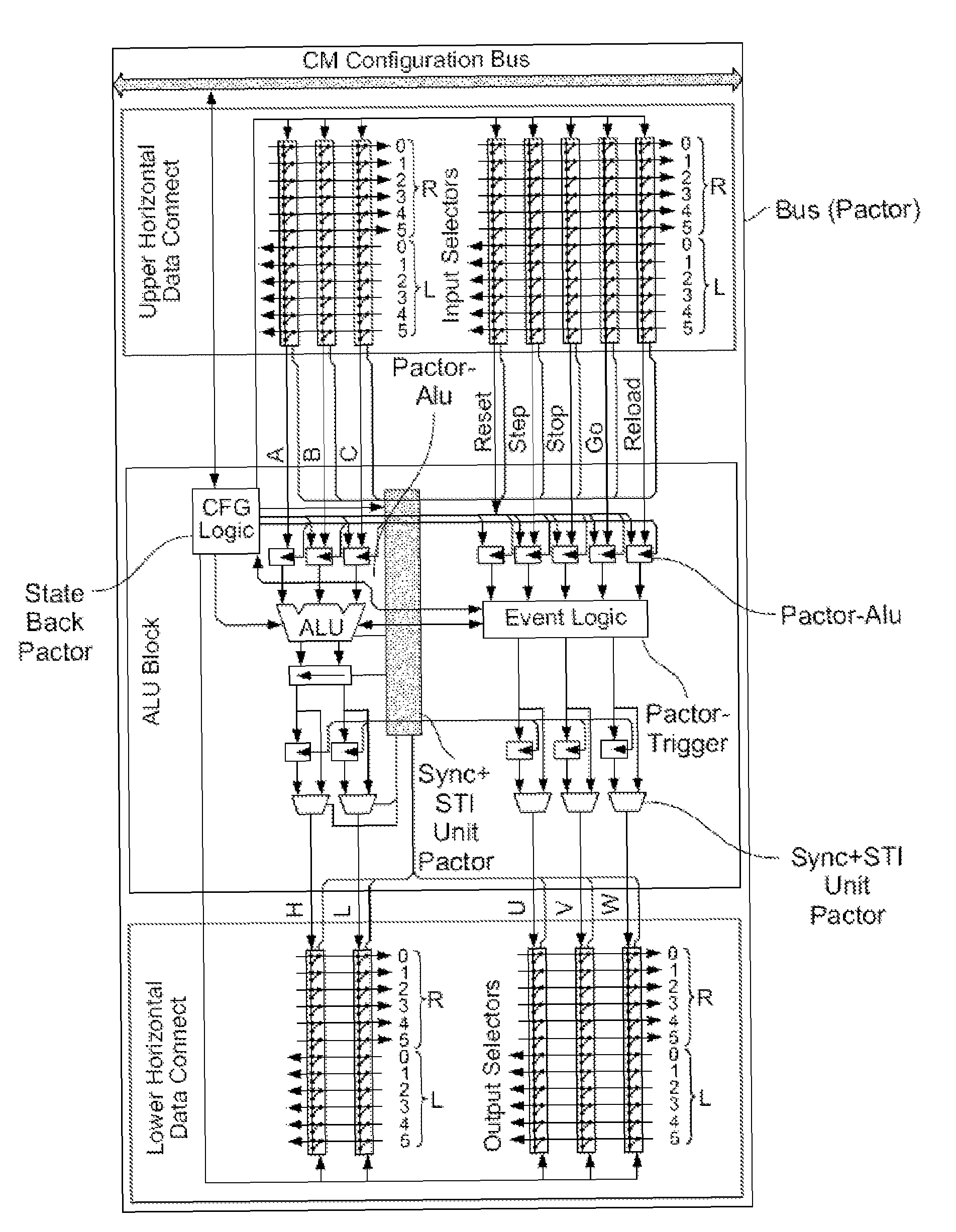
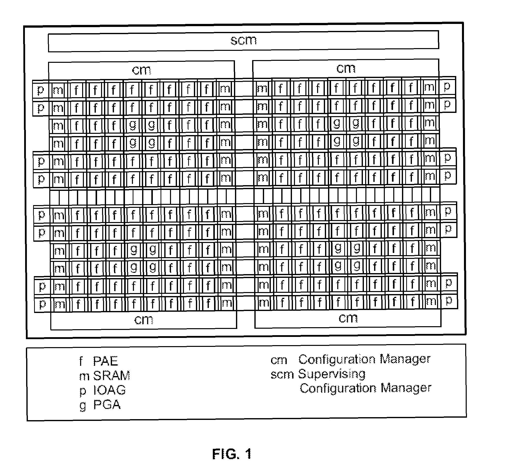
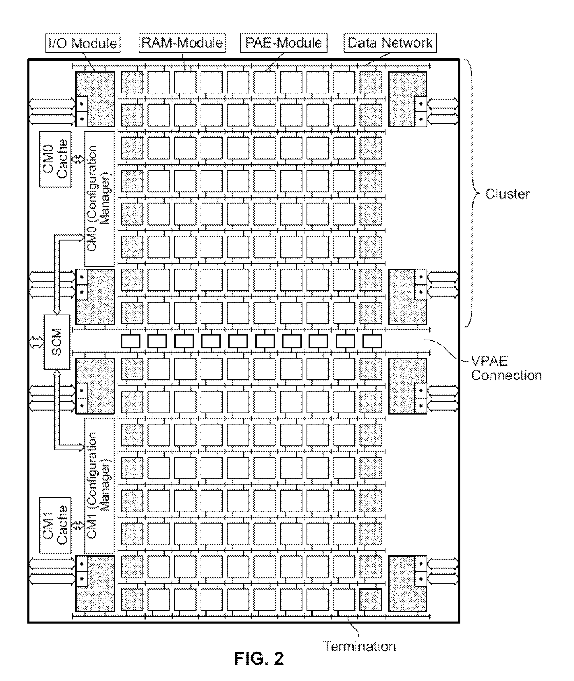
[0064]According to FIG. 1, a processor 1, which may form a unit that may be characterized as an XPP (extreme processing platform), includes two fields or clusters including: a number of arithmetic logic cells (ALU-PAE's=arithmetic logic unit processing array element); memory cells (RAM-PAE's=Random Access Memory processing array element); several illustrated as four input / output cells (I / O elements, input / output processing array element); a bus system running through each field; and a configuration manager that is assigned to the field, these elements together as a cluster forming a unit, which by itself is capable of processing data and doing so as a reconfigurable unit and a higher-order configuration manager being assigned to the two configuration managers (CM) of the cluster in order to form thereby a master cluster or the XPP. It is possible using tree-like hierarchical structures to have more than two fields of processor elements cooperate. In this manner, a higher-order confi...


PUM


Abstract

A logic cell array having a number of logic cells and a segmented bus system for logic cell communication, the bus system including different segment lines having shorter and longer segments for connecting two points in order to be able to minimize the number of bus elements traversed between separate communication start and end points.

Description

FIELD OF THE INVENTION[0001]The present invention relates to logic cell arrays.BACKGROUND INFORMATION[0002]Logic cell arrays, such as, for example, reconfigurable logic cell arrays include, as particular types, systolic arrays, neuronal networks, multi-processor systems, processors having a number of arithmetic-logic units, and / or logic cells and / or communicative / peripheral cells (I / O), networking and / or network chips, such as crossbar switches, as well as FPGA, DPGA, Xputer, Chameleon chips, etc. The following patents commonly assigned to the assignee of the present application describe logic cell arrays and are incorporated by reference in their entirety: German Patent No. 44 16 881; German Patent No. 197 81 412; German Patent No. 197 81 483; German Patent No. 196 54 846, German Patent No. 196 54 593; German Patent No. 197 04 044; German Patent No. 198 80 129, German Patent No. 198 61 088, German Patent No. 199 80 312; International Patent Application No. PCT / DE 00 / 01869; German P...

Claims


Application Information

Patent Timeline
Patent Type & Authority Patents(United States)
IPC IPC(8): H03K19/177G06F15/00G06F7/52G06F13/36G06F15/76G06F15/78
CPCG06F15/7867H03K19/17796
Inventor VORBACH, MARTINMAY, FRANKREICHARDT, DIRKLIER, FRANKEHLERS, GERDNUCKEL, ARMINBAUMGARTE, VOLKERRAO, PRASHANTOERTEL, JENS
Owner SCIENTIA SOL MENTIS AG
Why Eureka
Try Eureka