High voltage semiconductor device and method of manufacture thereof

a semiconductor and high-voltage technology, applied in the direction of semiconductor devices, basic electric elements, electrical apparatus, etc., can solve the problem of insufficient breakdown voltage in this portion, and achieve the effect of suppressing the lowering of breakdown voltage, reducing current crowding, and reducing current density

Inactive Publication Date: 2009-10-13
PANASONIC CORP
View PDF8 Cites 5 Cited by
  • Summary
  • Abstract
  • Description
  • Claims
  • Application Information

AI Technical Summary

Benefits of technology

[0016]Here, in an IGBT, to reduce the turnoff time inferior to the turnoff time of high breakdown voltage MOS transistor, the impurity concentration of the collector buffer layer may be set to be high, and as a result, electric field is further concentrated in the vicinity of the surface where the drift diffusion layer overlaps the collector buffer layer, and lowers breakdown voltage.
[0017]To solve the above-described problems, an object of the present invention is to provide an excellent high voltage semiconductor device that can improve the breakdown voltage of an element while maintaining short turn-off time, and a method of manufacture thereof.
[0024]By the high voltage semiconductor device and the method of manufacture thereof according to the present invention, since the impurity concentration in the second overlapped region in the corner portion is relatively low compared with the impurity concentration in the first overlapped region in the straight-line portion, the drift resistance component in the corner portion is relatively elevated, the current density is lowered, and current crowding is relieved. Therefore, an excellent high voltage semiconductor device that can suppress the lowering of breakdown voltage at on-time due to current crowding in the corner portion of the collector diffusion layer of the first conductivity type while maintaining a short turn-off time can be realized.
[0025]In the above-described high voltage semiconductor device, by isolating only the corner portion of the collector diffusion layer of the first conductivity type where current crowding easily occurs at on-time by an optional distance between the collector buffer layer of the second conductivity type and the low-concentration drift diffusion layer of the second conductivity type, current crowding is further relieved, and the lowering of breakdown voltage at on-time can also be suppressed.
[0026]Furthermore, in the IGBT, to limit the implantation of carriers from the collector diffusion layer of the first conductivity type, the collector buffer layer of the second conductivity type is formed so as to surround the collector diffusion layer of the first conductivity type. The impurity concentration of the collector buffer layer of the second conductivity type contacting the collector diffusion layer of the first conductivity type is set to be low so as to suppress current crowding on the surface, and immediately under the collector diffusion layer of the first conductivity type, the impurity concentration is set to be relatively high. As a result, the implantation of carriers from the collector diffusion layer of the first conductivity type can be controlled, and the turn-off time can be shortened.
[0027]In conventional examples, the drift diffusion layer wherein a current flows is formed on the surface, and since the peak of impurity concentration is in the vicinity of the surface, the current flows in the vicinity of the surface. It is considered that electric fields are also concentrated in the vicinity of the surface, and thus if the concentration of the drift diffusion layer is elevated, breakdown voltage at off-time is also lowered. However in the present invention, such defects can be avoided. In the invention described in Japanese Patent No. 3730283, although application to IGBT is also proposed, the dose in the collector buffer layer of the second conductivity type is 10×1013 to 2.5×1013 cm−2, and the turnoff time is about 0.5 μsec. On the other hand in the present invention, since the impurity concentration on the surface can be suppressed to be low to relieve current crowding, the dose can be set to be higher than the dose in the invention described in Japanese Patent No. 3730283. As a result, the turnoff time can be shortened.

Problems solved by technology

However, when positive bias relative to the emitter is supplied to the collector, since the collector buffer layer has relatively high impurity concentration, equipotential lines are crowded in the vicinity of the collector buffer layer, and there is possibility that breakdown voltage is insufficient in this portion.

Method used


Image

  • High voltage semiconductor device and method of manufacture thereof
  • High voltage semiconductor device and method of manufacture thereof
  • High voltage semiconductor device and method of manufacture thereof

Examples


first embodiment

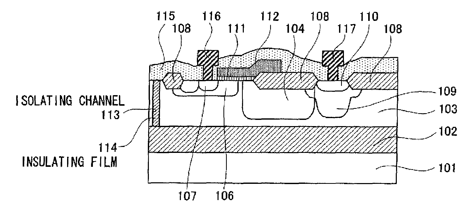
[0045]An IGBT, which is a high voltage semiconductor device according to a first embodiment of the present invention, will be described referring to the drawings.

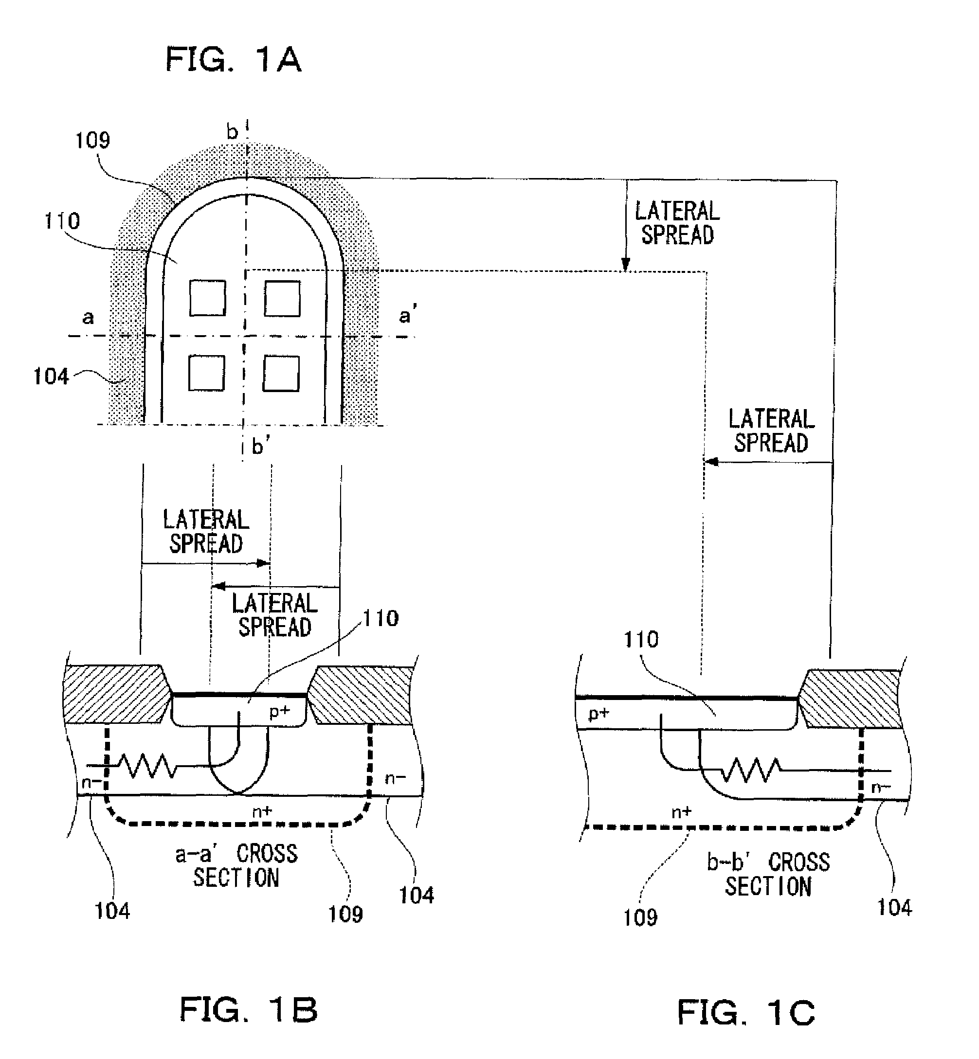
[0046]FIG. 1A is a plan structural diagram illustrating that an n+-type collector buffer layer 109 is formed on a p-type silicon layer 103 adjacent to an n−-type drift diffusion layer 104 in the IGBT of the present invention. FIGS. 1B and 1C are cross-sectional structural diagrams along the line a-a′ and the line b-b′ in FIG. 1A, respectively.

[0047]The present invention differs from the conventional examples in that in the conventional examples, an n-type drift diffusion layer 104 is formed so as to completely include the region of an n+-type collector buffer layer 109, whereas in the IGBT of the present invention shown in FIGS. 1A to 1C, an n−-type drift diffusion layer 104 is formed so as to surround the n+-type collector buffer layer 109. Since other structures are basically identical to those in the conventional example...

second embodiment

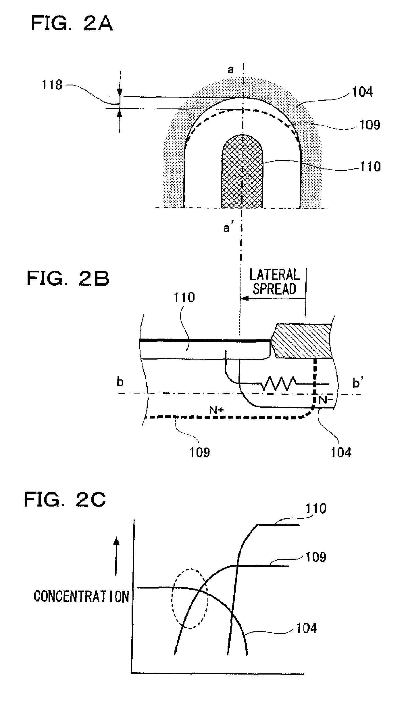
[0052]Next, an IGBT, which is a high voltage semiconductor device according to a second embodiment of the present invention, will be described referring to the drawings.

[0053]FIG. 2A is a plan structural diagram of an IGBT, which is the high voltage semiconductor device according to the second embodiment of the present invention; FIG. 2B is a cross-sectional structural diagram along the line a-a′ in FIG. 2A; and FIG. 2C is a graph showing an impurity concentration profile of the n+-type collector buffer layer 109 and the n−-type drift diffusion layer 104 in the vicinity of the line b-b′ in FIG. 2B.

[0054]The IGBT in the second embodiment has a structure and components identical to those of the IGBT in the first embodiment shown in FIGS. 1A and 1B except the location of the n−-type drift diffusion layer 104 relative to the p+-type collector diffusion layer 110 and the n+-type collector buffer layer 109. Therefore, the description for the same components will be omitted by using the sa...

third embodiment

[0058]Next, an IGBT, which is a high voltage semiconductor device according to a third embodiment of the present invention, will be described referring to the drawings.

[0059]FIG. 3A is a plan structural diagram of the IGBT, which is the high voltage semiconductor device according to the third embodiment of the present invention; FIG. 3B is a cross-sectional structural diagram along the line a-a′ in FIG. 3A; and FIG. 3C is a graph showing an impurity concentration profile of the n+-type collector buffer layer 109 and the n−-type drift diffusion layer 104 in the vicinity of the line b-b′ in FIG. 3B.

[0060]The IGBT in the third embodiment has a structure and components identical to those of IGBTs in the first and second embodiments shown in FIGS. 1 and 2 except the location of the n+-type collector buffer layer 109 relative to the p+-type collector diffusion layer 110. Therefore, the description for the same components will be omitted by using the same reference numerals and characters ...


PUM


Abstract

A drift diffusion layer of a low concentration is formed so as to surround a collector buffer layer having a relatively high concentration including a high-concentration collector diffusion layer in a plane structure. Thereby, current crowding in corner portions of the high-concentration collector diffusion layer is suppressed while maintaining a short turnoff time, and the improvement of breakdown voltage at on-time is realized.

Description

FIELD OF THE INVENTION[0001]The present invention relates to a high voltage semiconductor device and a method of manufacture thereof, and more specifically to an insulated gate bipolar transistor (hereafter abbreviated as “IGBT”) that realizes high breakdown voltage while maintaining a short turnoff time and a low on-voltage.BACKGROUND OF THE INVENTION[0002]For isolating elements in a semiconductor device, a large number of junction isolating techniques using p-n junction have been used for a long time. In recent years, however, dielectric isolation wherein in an SOI (silicon on insulator) substrate having a buried insulating film, a trench that extends from the surface of the substrate to the buried insulating film is formed, and an insulating film is formed in the trench, has been used.[0003]Such an element structure of SOI-trench isolation is especially effective in semiconductor devices for high breakdown voltage power fields wherein the formation of deep isolation is generally ...

Claims


Application Information

Patent Timeline
Patent Type & Authority Patents(United States)
IPC IPC(8): H01L29/739H01L21/332
CPCH01L29/7394H01L29/66325
Inventor NISHIMURA, HISAJIOGURA, HIROYOSHIOHDAIRA, AKIRA
Owner PANASONIC CORP
Why Eureka
Try Eureka