Piezoelectric device, its manufacturing method, and touch panel device

a piezoelectric device and manufacturing method technology, applied in static indicating devices, generators/motors, instruments, etc., can solve the problems of low electromechanical conversion efficiency of piezoelectric devices and particularly prone to production/growth of hillocks, so as to improve detection precision, reduce driving voltage, and high electromechanical conversion efficiency

Inactive Publication Date: 2009-10-20
FUJITSU LTD
View PDF16 Cites 8 Cited by
  • Summary
  • Abstract
  • Description
  • Claims
  • Application Information

AI Technical Summary

Benefits of technology

[0012]From hitherto, the piezoelectric film in prescribed piezoelectric devices has been formed by depositing a piezoelectric material by sputtering, with the substrate being heated during the deposition. When the substrate is heated, each electrode already formed on the substrate (e.g. the IDT of a conventional piezoelectric device as described above) is heated together with the substrate, and hence due to a difference in the thermal expansion coefficient between the substrate and the electrode, hillocks (parts where the electrode peels away from the surface of the substrate) arise on the electrode. It is known that the more numerous such hillocks or the larger such hillocks, the lower the electromechanical conversion efficiency in the piezoelectric device. With a conventional piezoelectric device in a SAW type touch panel device, Al is often used as the material for constituting the IDT (electrodes). This is because Al has low electrical resistance, is cheap, and is easily processed. However, production / growth of hillocks is particularly prone to occur with such an Al electrode.
[0027]At least one of the exciting means and the receiving means of the touch panel device having this constitution is constituted from a piezoelectric device having a high electromechanical conversion efficiency according to the first aspect of the present invention. The touch panel device according to the sixth aspect of the present invention is thus suitable in terms of reducing the driving voltage or improving the detection precision.

Problems solved by technology

It is known that the more numerous such hillocks or the larger such hillocks, the lower the electromechanical conversion efficiency in the piezoelectric device.
However, production / growth of hillocks is particularly prone to occur with such an Al electrode.

Method used


Image

  • Piezoelectric device, its manufacturing method, and touch panel device
  • Piezoelectric device, its manufacturing method, and touch panel device
  • Piezoelectric device, its manufacturing method, and touch panel device

Examples


example 1

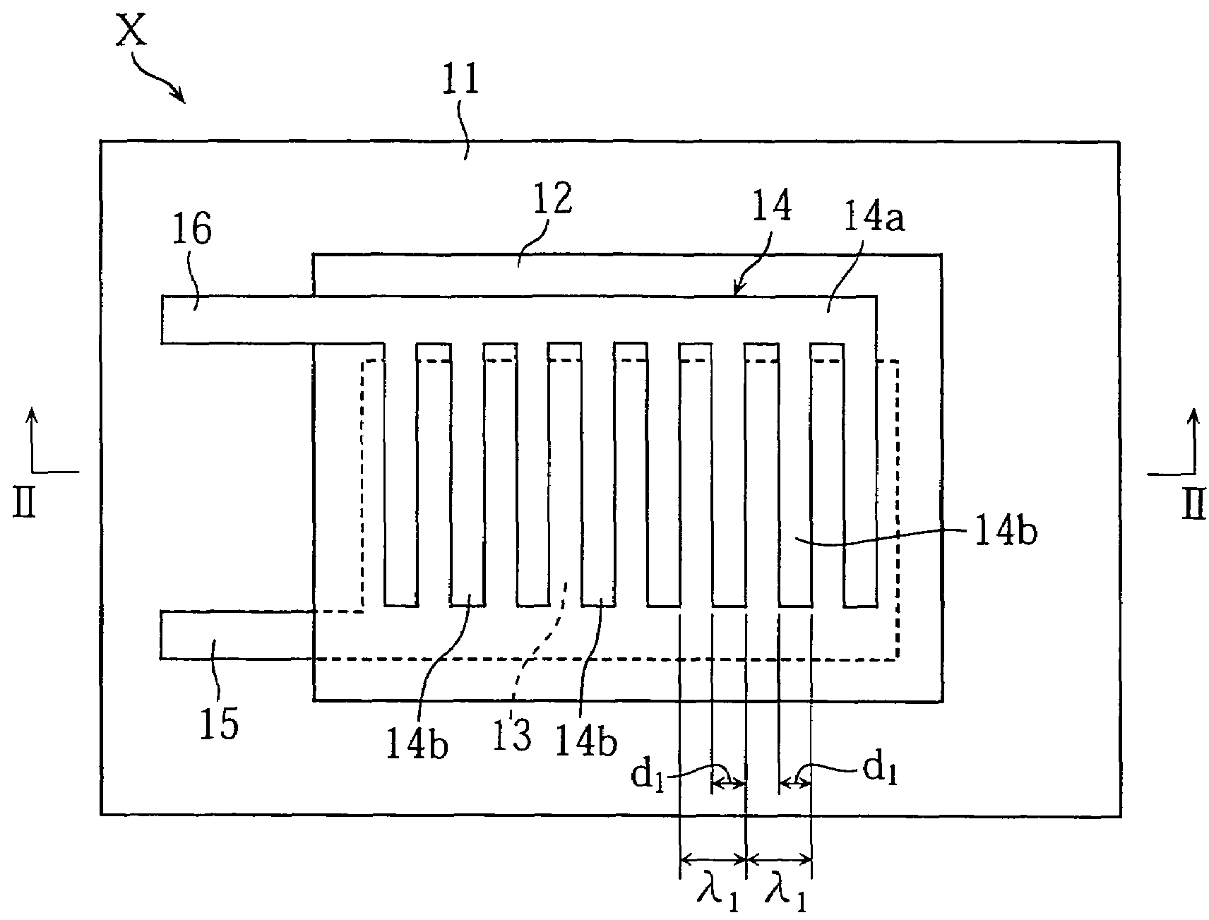
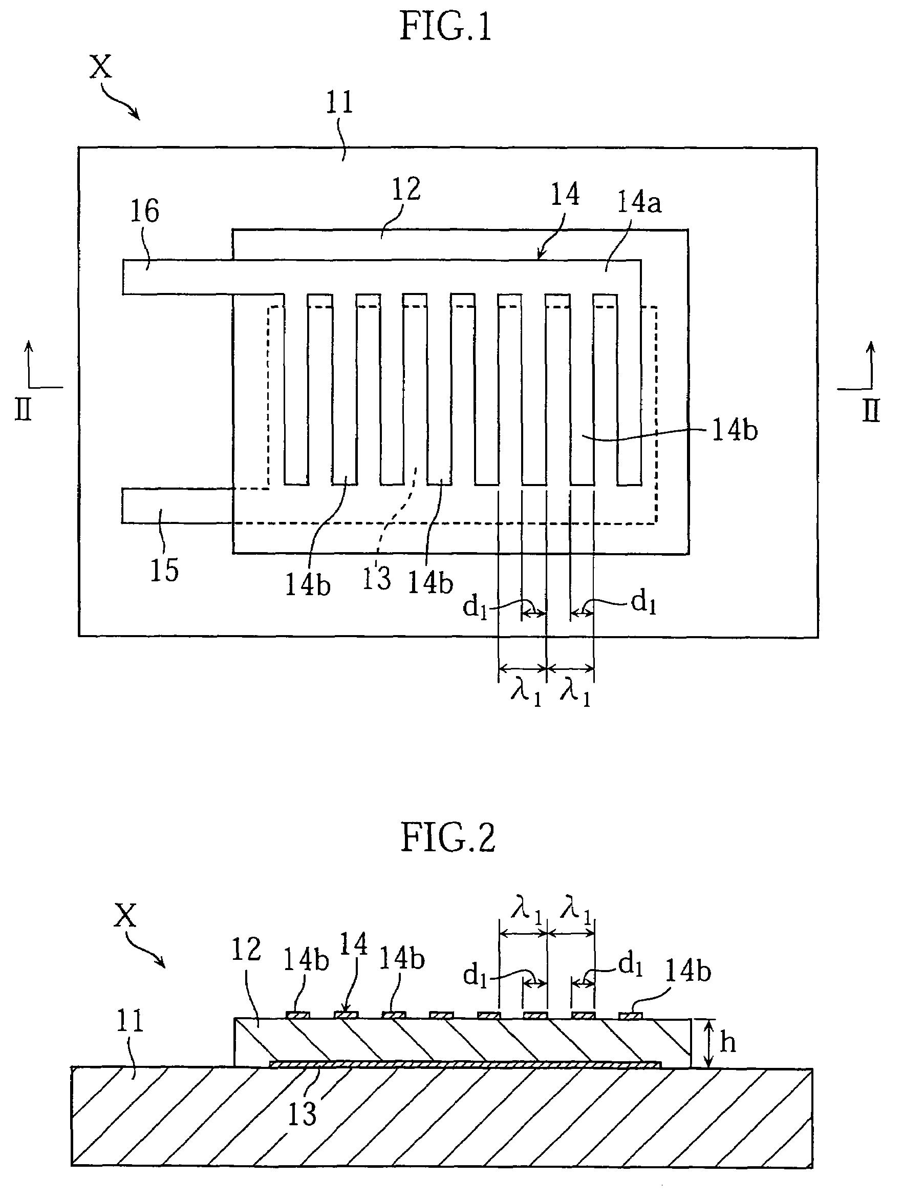
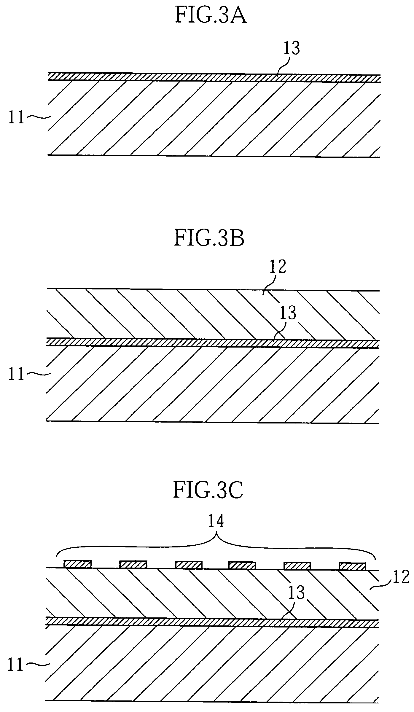
[0106]A normal facing type filter comprising two piezoelectric devices X as shown in FIG. 11 was manufactured. Each of the piezoelectric devices X constituting the filter of the present example was a piezoelectric device X according to the first embodiment. In the manufacture of the filter, first, in a first film formation step, an Al alloy containing 1.0 wt % of Cu was deposited on a glass substrate 11 by sputtering, thus forming a 300 nm-thick Al alloy film. In the sputtering, a target of an Al alloy containing 1.0 wt % of Cu was used.

[0107]Next, the Al alloy film was etched with a prescribed resist pattern as a mask, thus patterning the Al alloy film. In this way, electrodes 13 and terminals 15 were formed on the substrate 11. After that, the surface of each of the electrodes 13 was subjected to etching treatment by reverse sputtering using an Ar plasma.

[0108]Next, in a second film formation step, ZnO was deposited on the substrate 11 by sputtering, thus forming a 2 μm-thick piez...

example 2

[0111]A plurality of filters according to the present example were manufactured using the same method as for Example 1, except that an Al alloy containing 0.5 wt % of Cu was deposited in the first film formation step instead of the Al alloy containing 1.0 wt % of Cu. For the filters of the present example, each of the electrodes 13 thus comprised an Al alloy containing 0.5 wt % of Cu. Moreover, for all of the filters of the present example, the thickness h of each of the piezoelectric films 12 was 2 μm, and hence this thickness h and the electrode period λ1 of the branch electrodes 14b satisfied the condition 0.005≦h / λ1≦0.1.

example 3

[0112]A plurality of filters according to the present example were manufactured using the same method as for Example 1, except that an Al alloy containing 2.0 wt % of Cu was deposited in the first film formation step instead of the Al alloy containing 1.0 wt % of Cu. For the filters of the present example, each of the electrodes 13 thus comprised an Al alloy containing 2.0 wt % of Cu. Moreover, for all of the filters of the present example, the thickness h of each of the piezoelectric films 12 was 2 μm, and hence this thickness h and the electrode period λ1 of the branch electrodes 14b satisfied the condition 0.005≦h / λ1≦0.1.


PUM

PropertyMeasurementUnit
thicknessaaaaaaaaaa
thicknessaaaaaaaaaa
thicknessaaaaaaaaaa

Abstract

A piezoelectric device (X) includes a substrate (11) a piezoelectric film (12), a first electrode (13), and a second electrode (14). At least one of the first electrode (13) and the second electrode (14) is interposed between the substrate (11) and the piezoelectric film (12), and made of an Al alloy containing 0.1 to 3 wt % of at least one metal selected from the group consisting of Ti, Cr, Ni, Cu, Zn, Pd, Ag, Hf, W, Pt and Au.

Description

[0001]This application is a continuing application, filed under 35 U.S.C. § 111(a), of International Application PCT / JP2003 / 006425, filed May 22, 2003.TECHNICAL FIELD[0002]The present invention relates to a piezoelectric device able to excite surface acoustic waves, and a manufacturing method thereof, and also a touch panel device having such piezoelectric devices as exciting means and receiving means.BACKGROUND ART[0003]Touch panel devices are sometimes used as means for inputting into computer systems in FA equipment, OA equipment, measuring equipment and so on. Touch panel devices are generally provided on the display of the equipment, and are for detecting the position where a finger or the like has contacted the surface of the display. Prescribed processing is carried out in the computer system of the equipment based on data relating to images displayed on the display and data relating to the position of contact detected by the touch panel device.[0004]In the technical field of...

Claims


Application Information

Patent Timeline
Patent Type & Authority Patents(United States)
IPC IPC(8): H01L41/08G09G5/00G06F3/041H01L41/047H01L41/22H01L41/29
CPCG06F3/0436H01L41/0477H01L41/29H01L41/0805H01L41/316H10N30/877H10N30/1051H10N30/06H10N30/076
Inventor KATSUKI, TAKASHINAKAZAWA, FUMIHIKOSANO, SATOSHITAKAHASHI, YUJI
Owner FUJITSU LTD
Why Eureka
Try Eureka