Plasma display panel and display employing the same having transparent intermediate electrodes and metal barrier ribs

Inactive Publication Date: 2009-10-20
HITACHI LTD
View PDF21 Cites 6 Cited by
  • Summary
  • Abstract
  • Description
  • Claims
  • Application Information

AI Technical Summary

Benefits of technology

[0023]The present invention has been made in view of those problems in the prior art and it is therefore an object of the present invention to provide a plasm

Problems solved by technology

Therefore, the plasma display panel cannot be satisfactorily grounded, discharges in the panel are unstable, and undesired electromagnetic radiation that affects adversely to the nearby drive circuit occurs.
However, if the distances between the display electrodes 2 and 3 are not sufficiently long, the discharge mode of glow discharge has difficulty in forming a positive column region that produces ultraviolet rays effectively, and most part of the glow discharge is a negative glow region.
Since the barrier ridges 9 shown in FIG. 12 are dielectric, charged particles produced by a discharge diffuse into the barrier ribs 9, causing loss that reduces luminous efficiency.
The current needs to be increased to sustain a discharge, which reduces the efficiency of positive columns.
However, the low driving current reduces luminance for one pulse.

Method used


Image

  • Plasma display panel and display employing the same having transparent intermediate electrodes and metal barrier ribs
  • Plasma display panel and display employing the same having transparent intermediate electrodes and metal barrier ribs
  • Plasma display panel and display employing the same having transparent intermediate electrodes and metal barrier ribs

Examples


first embodiment

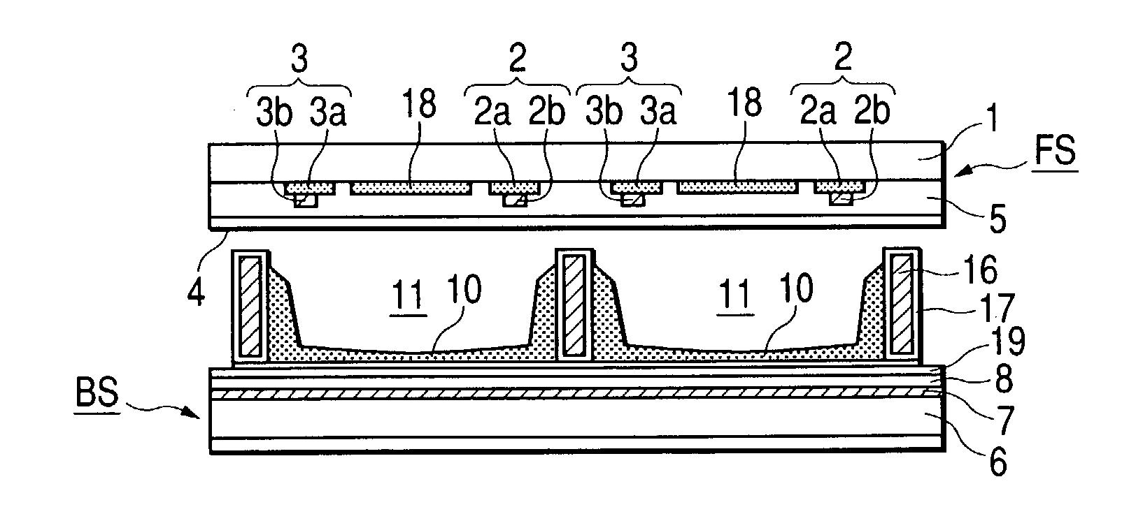
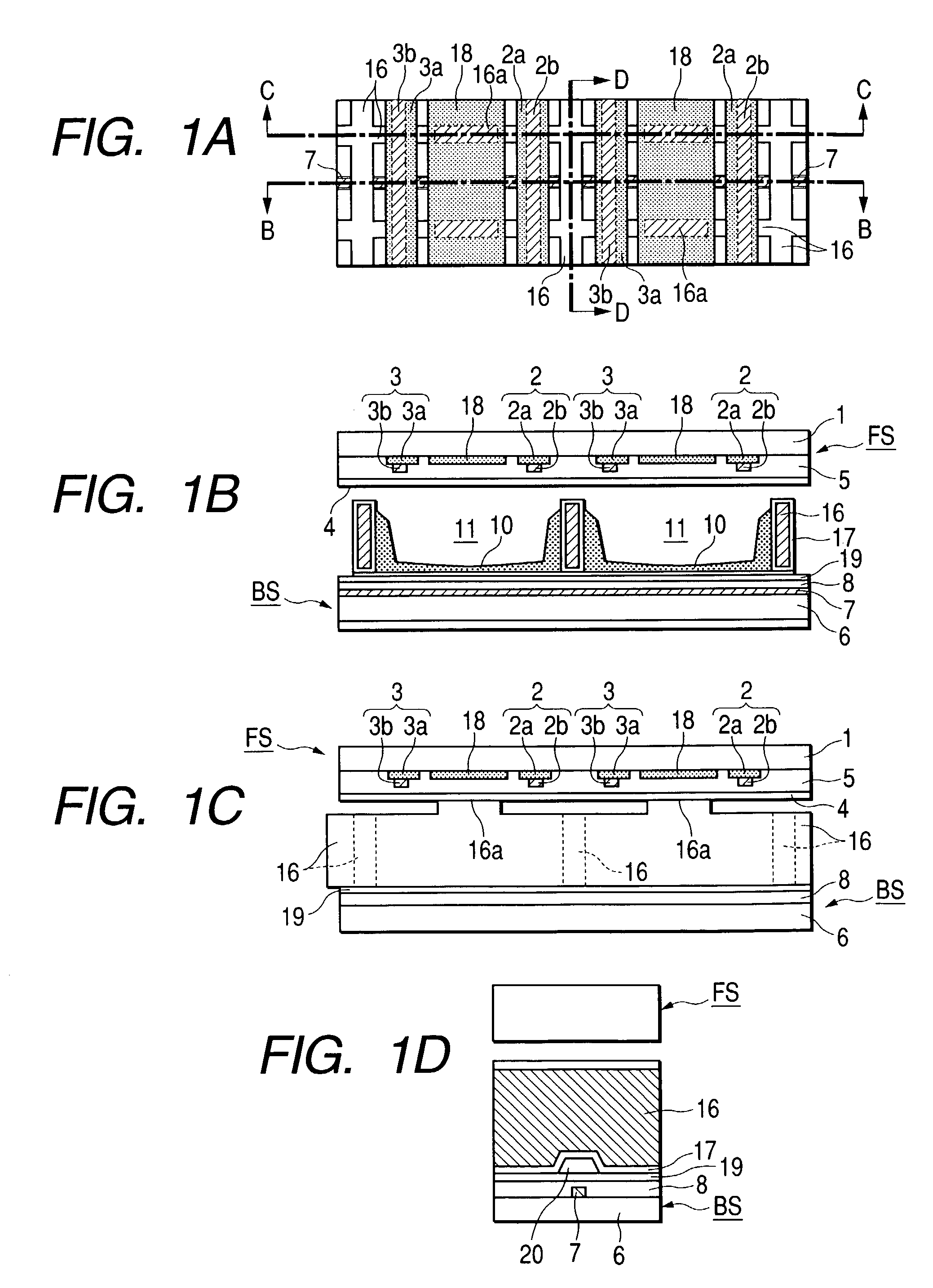
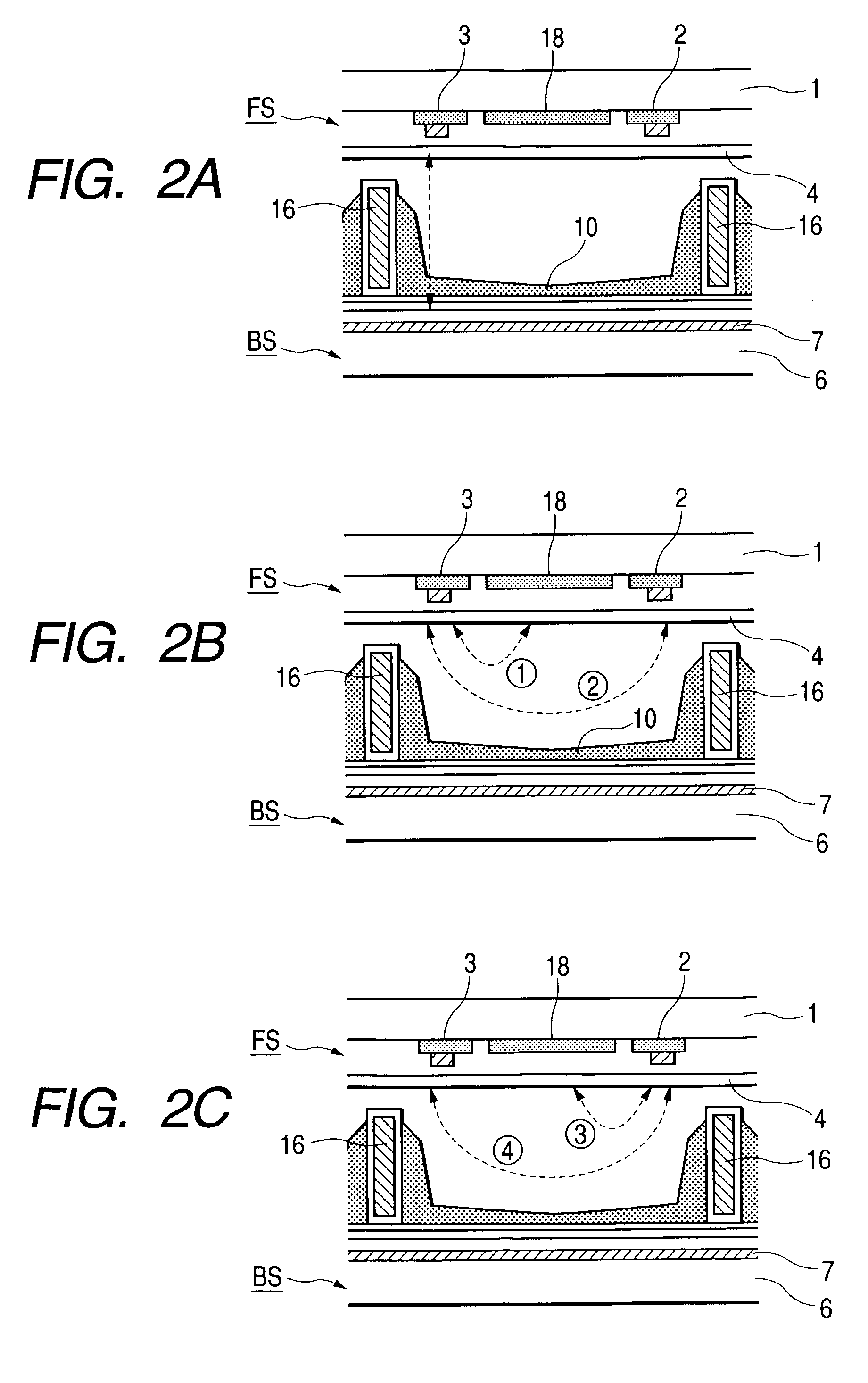
[0050]FIG. 1A is a plan view of plasma display panel in a first embodiment according to the present invention as viewed from the side of a front panel. FIGS. 1B, 1C and 1D are sectional views taken on line B-B, line C-C and line D-D, respectively, in FIG. 1A. Shown in FIGS. 1A to 1D are metal barrier ribs 16, projections 16a projecting from the metal barrier ribs 16, intermediate electrodes 18, a protective layer 19 of an MgO film or such, and a hollow 20. In FIGS. 1A to 1D, parts like or corresponding to those shown in FIGS. 12 and 16 are denoted by the same reference characters and the description thereof will be omitted to avoid duplication.

[0051]Referring to FIG. 1, the metal barrier ribs 16 are formed by making through holes corresponding to discharge spaces 11 for cells in a thin plate of an Fe—Ni alloy having a coefficient of thermal expansion substantially equal to those of glass substrates 1 and 6 by an etching process or the like. As shown in FIG. 1B, all the surfaces of t...

second embodiment

[0076]FIG. 5 shows a plasma display panel in a second embodiment according to the present invention, in which FIG. 5A is a plan view taken from the side of a front glass substrate, FIG. 5B is a longitudinal sectional view taken on line B-B in FIG. 5A, and FIG. 5C is a longitudinal sectional view taken on line C-C in FIG. 5A. Shown in FIGS. 5A to 5C are a protective layer 5′, a conductive layer 24 and projections 25. In FIGS. 5A to 5C, parts like or corresponding to those shown in FIGS. 1A to 1D are denoted by the same reference characters and the description thereof will be omitted to avoid duplication.

[0077]Referring to FIG. 5B, which corresponds to FIG. 1B, a dielectric layer 5 is formed on a surface facing metal barrier ribs 16 of a front substrate FS, and the dielectric projections 25 are formed on the dielectric layer 5 along the metal barrier ribs 16 for each cell. The plasma display panel in the second embodiment is the same in other respects as that in the first embodiment. ...

third embodiment

[0080]FIG. 6 is a typical sectional view of an essential part around a metal barrier rib 16 of a plasma display panel in a third embodiment according to the present invention, in which parts like or corresponding to those shown in FIG. 5 are denoted by the same reference characters and the description thereof will be omitted.

[0081]Referring to FIG. 6, projections are formed along thee metal barrier rib 16 in parts corresponding to intersections of intermediate electrodes 18 and the metal barrier ribs 16 of a surface of a front substrate FS. Each projection consists of a conductive layer 27, and a part corresponding to the conductive layer 27 of a dielectric layer 26 covering the conductive layer 27. A conductive layer 24 is formed on the intermediate electrode 18 similarly to the conductive layer 24 of the second embodiment shown in FIG. 5C. The conductive layers 24 and 27 further enhances the capacitive coupling of the intermediate electrode 18 and the metal barrier rib 16 and the ...


PUM


Abstract

An intermediate electrode is formed in a space between an X display electrode and a Y display electrode parallel thereto. A negative voltage is applied to the Y display electrode to use the Y display electrode as a cathode. A charge is stored between the Y display electrode and an intermediate electrode to create an electric field. Upon the increase of the intensity of the electric field to a sufficiently high level, an instant discharge occurs between the Y display electrode and the X display electrode and intense ultraviolet rays are produced. The fluorescent layer excited by the ultraviolet rays emits visible light. Only a narrow pulse current flows through the X display electrode and the Y display electrode, so that power consumption can be suppressed at high emission efficiency.

Description

BACKGROUND OF THE INVENTION[0001]1. Field of the Invention[0002]The present invention relates to a plasma display panel for a use in information processing terminals and flat wall television sets, and a display employing the same. In particular, the present invention relates to a plasma display panel capable of operating at greatly improved luminous efficiency and of displaying images in greatly improved luminance, and to a display employing the same.[0003]2. Description of the Related Art[0004]A reflective three-electrode surface discharge plasma display panel provided with two kinds of transparent display electrodes formed on the same surface of a front substrate is used prevalently. A prior art reflective three-electrode surface discharge plasma display panel is disclosed in JP 10-207419A.[0005]Referring to FIG. 12 showing part of the known plasma display in a perspective view, there are shown a front substrate FS, a back substrate BS, a front glass substrate 1, an X display elec...

Claims


Application Information

Patent Timeline
IPC IPC(8): G09G3/28G09G3/20G09G3/288G09G3/291G09G3/292G09G3/293G09G3/294G09G3/296H01J11/12H01J11/16H01J11/22H01J11/24H01J11/26H01J11/30H01J11/32H01J11/34H01J11/38H01J11/42H04N5/66
CPCG09G3/2022G09G3/2927G09G3/2932G09G3/2935G09G3/2942G09G3/2986H01J11/12H01J11/28H01J11/32H01J11/36H01J2211/366G09G2320/0238H01J2211/326G09G2320/0228G09G3/296H01J11/34
Inventor AKIBA, YUTAKA
Owner HITACHI LTD
Why Eureka
Try Eureka