

Continuous clocking of TDI sensors
a technology of tdi sensors and continuous clocking, which is applied in the field of electromechanical imaging, can solve the problems of sensor high power dissipation, tdi sensors that employ burst clocking do not exhibit optimal speed in transferring pixel charge, and tdi sensors that employ burst clocking do not exhibit optimal functionality
- Summary
- Abstract
- Description
- Claims
- Application Information
AI Technical Summary
Benefits of technology
Problems solved by technology
Method used
Image

Examples
Embodiment Construction
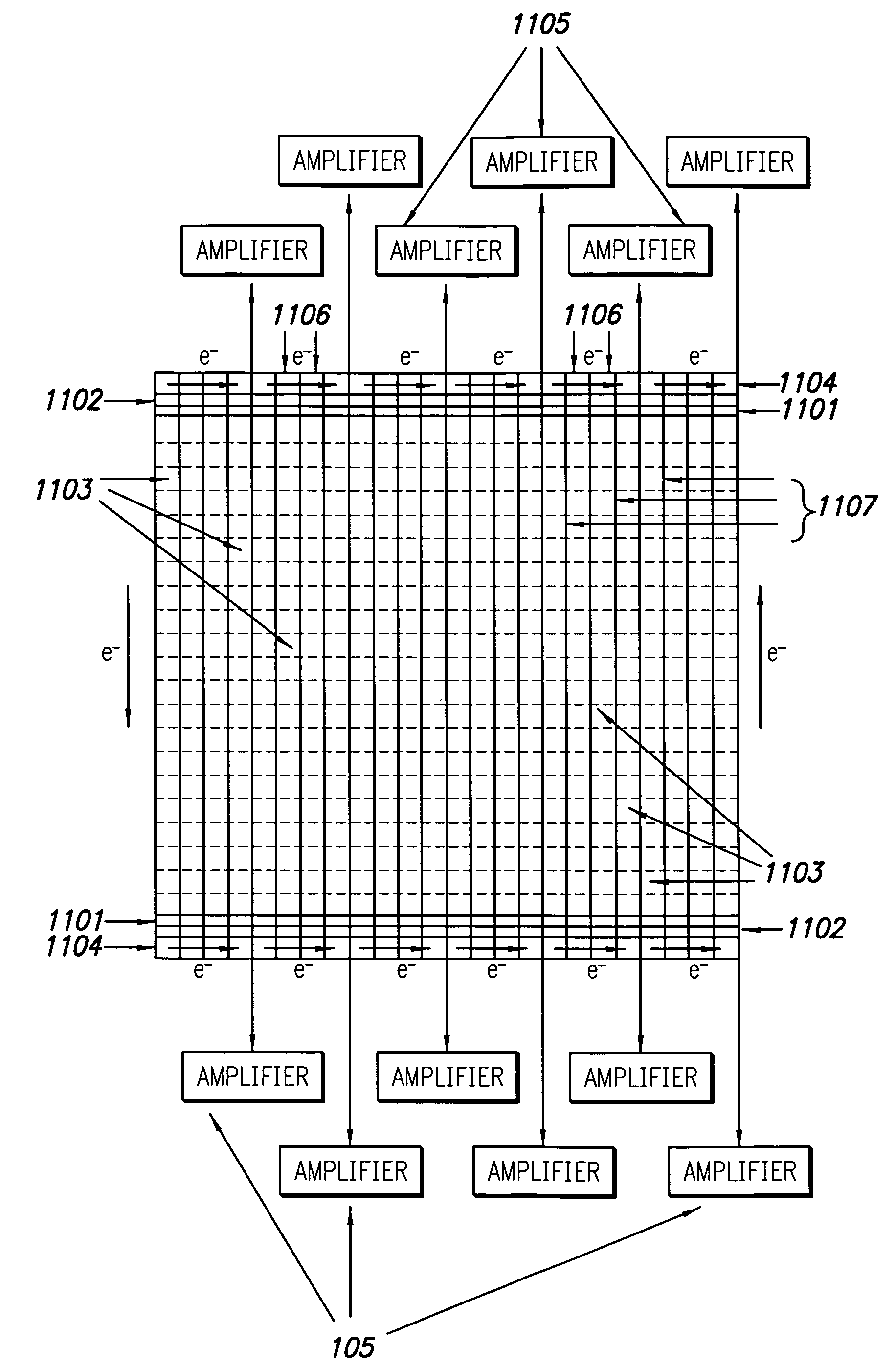
[0031]According to the present invention, there is provided a TDI sensing arrangement, potentially for use in an inspection system that employs continuous clocking to transfer charge between pixels. The present design may offer improvements over previously known TDI sensor designs.
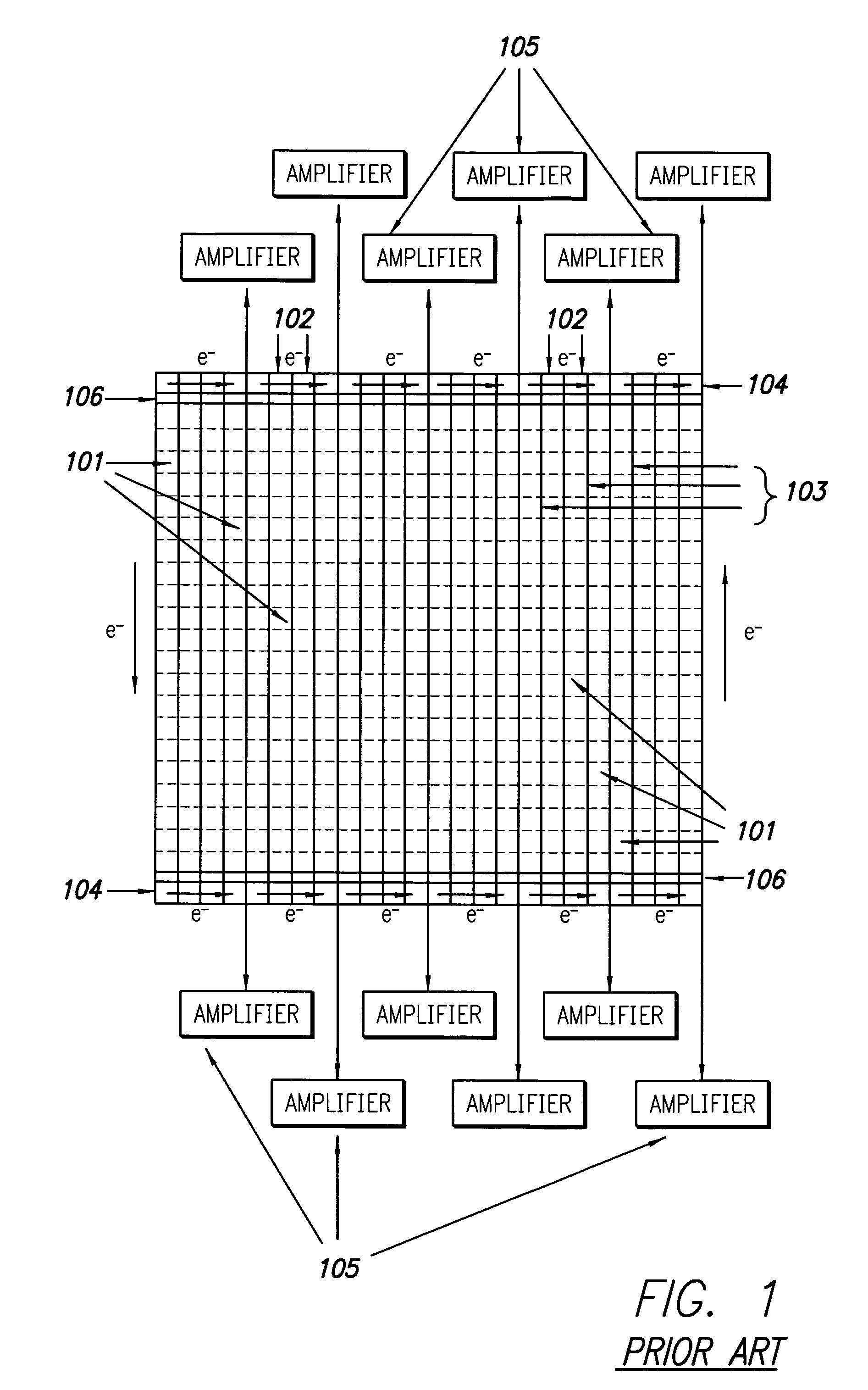
Burst Clocking
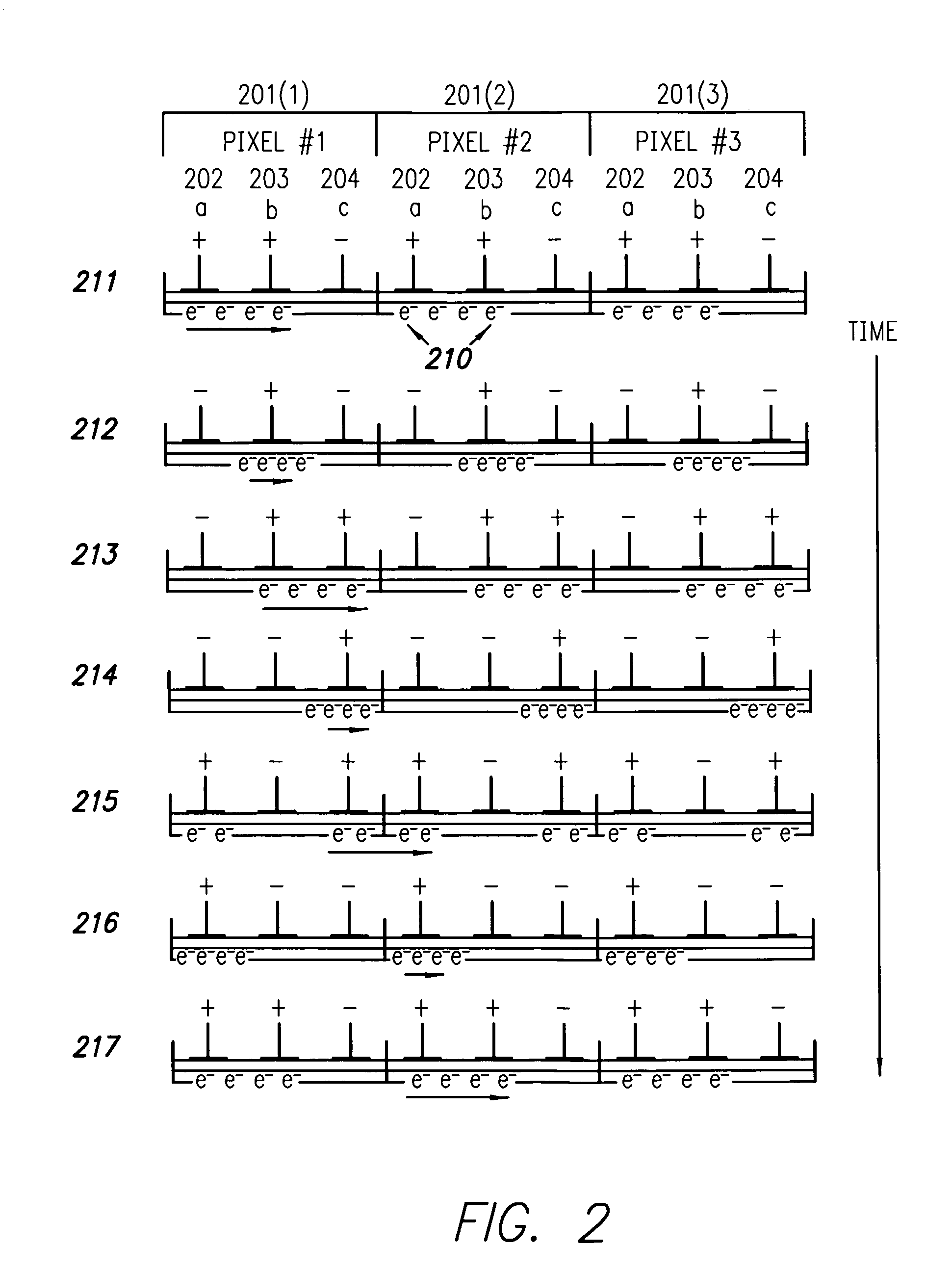
[0032]FIG. 2 illustrates how previous TDI sensors move charge from one pixel to another within a column of pixels. FIG. 2 shows three neighboring pixels 201(1), 201(2), and 201(3) within a single column. The term “column” relating to FIG. 2 serves to explain how the charge moves vertically from pixel to pixel in FIG. 1. Each pixel comprises three polysilicon gates, labeled a 202, b 203, and c 204. This three-gate structure enables the charge to move in the desired direction.
[0033]FIG. 2 illustrates three pixels, each with three gates, in seven different states 211-217. In this example, the initial state of the TDI sensor is state 211. The TDI sensor advances to states 212, 213, and so forth s...
PUM
| Property | Measurement | Unit |
|---|---|---|
| diameter | aaaaa | aaaaa |
| size | aaaaa | aaaaa |
| gate voltage | aaaaa | aaaaa |
Abstract
Description
Claims
Application Information