

DC-DC converter and method of controlling thereof
a dc-dc converter and converter technology, applied in the direction of electric variable regulation, process and machine control, instruments, etc., can solve the problems of reducing the efficiency of the converter, unable to obtain the dc output voltage desirable for a dc-dc converter, incomplete essential on-off operation of the switching element 102, etc., to reduce the intermittent failure of the pwm signal
- Summary
- Abstract
- Description
- Claims
- Application Information
AI Technical Summary
Benefits of technology
Problems solved by technology
Method used
Image

Examples
first embodiment
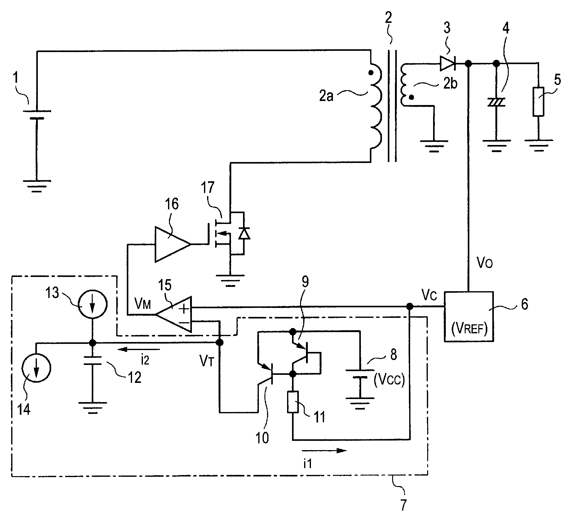
[0018]FIG. 1 is a circuit diagram showing a circuit configuration of a DC-DC converter according to the present invention. The DC-DC converter has a transformer 2 having a primary winding 2a and a secondary winding 2b. The primary winding 2a is connected to a positive electrode of a DC power source 1, and the secondary winding is connected to a diode 3, which is connected to a capacitor 4 and a load 5. An output voltage detecting and adjusting circuit 6 is connected to the diode 3, the capacitor 4, and the load. The circuit 6, like the output voltage detecting and adjusting circuit 108 in FIG. 5, outputs a command value VC based on a comparison between an output voltage VO of the converter and a reference value VREF.
[0019]Reference numeral 7 denotes a triangular generating circuit for generating a triangular wave VT on the basis of the command value VC. The triangular generating circuit 7 has a reference power source 8 (with a power source voltage taken as VCC), two transistors 9 an...
second embodiment
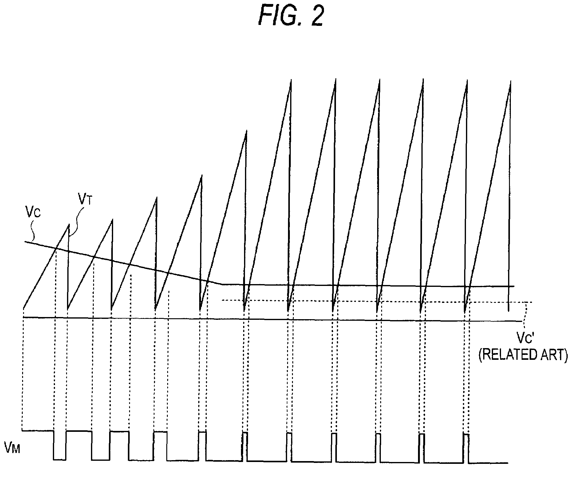
[0026]In the second embodiment, the voltage generated across the resistor 20 at turning ON operation of the switching element 17 is converted to current by the current converting circuit 19, by which the capacitor 12 is charged. With the voltage wave form of the capacitor 12 taken as a triangular wave VT, the voltage is compared with the command value VC by the comparator 15, by which an operation like that in the embodiment shown in FIG. 1 can be carried out. Namely, reducing the command value VC increases the current i2 flowing in the transistor 10 to increase the voltage superimposed on the voltage across the capacitor 12 in the same way as that described in the foregoing to result in more abrupt inclination of the triangular wave VT. Therefore, reducing the output voltage VO increases the command value VC to thereby allow the PWM signal VM to prevent intermittent failures.
[0027]FIG. 4 shows a circuit diagram showing a modified circuit configuration of the first embodiment. This ...
PUM
 Abstract
Description
Claims
Application Information