Method and apparatus for improving and controlling dynamic range in an image sensor

a dynamic range and image sensor technology, applied in the field of imaging sensors, can solve the problems of complex active-pixel circuit of cmos, lower quantum efficiency, higher fixed pattern noise, etc., and achieve the effect of enhancing the efficacy of dynamic range enrichmen

Active Publication Date: 2009-11-10
SAMSUNG ELECTRONICS CO LTD
View PDF17 Cites 12 Cited by
  • Summary
  • Abstract
  • Description
  • Claims
  • Application Information

AI Technical Summary

Benefits of technology

[0010]A method and apparatus for an electronic image sensor having a base exposure, followed by a second or multiple exposures that are formed during signal readout, before a next row is read. A timing controller controls the signal readout, such that as each line is read, the second and subsequent exposures are subsequently added to the base exposure to enrich the dynamic range. The image sensor may further include an analog-to-digital converter and noise suppression to further enhance the efficacy of the dynamic range enrichment. The system may also include additional signal processing and scaling functions.
[0011]In one embodiment, a method for enhancing the dynamic range of an electronic image sensor, the image sensor having rows of pixels, comprises processing a pixel signal over a first integration period to form a first signal sample for each pixel in a current row; reading the first signal sample for each pixel in the current row, on a row-by row basis; storing the first signal samples from the current row of the imaging sensor in a memory; processing the pixel signal for each pixel in the current row over a second integration period, prior to reading the first signal samples of a next row, to form a second signal sample of each pixel in the current row; and combining the first and second signal sample for each pixel of the first row to produce an enhanced signal, thereby enhancing the dynamic range of the image sensor.
[0016]For operation with an image sensor utilizing a global shutter, the first signal sample is formed for each pixel in the sensor during a main exposure using a global shutter, and then each pixel in each row is enhanced by forming the second signal sample during signal readout of each row.
[0021]The present invention may be utilized with an image sensor utilizing a global shutter, wherein the first signal is formed for each pixel in the sensor during a main exposure using a global shutter, and then each pixel in each row is enhanced by forming the second signal during signal readout of each row.

Problems solved by technology

Complicated CMOS active-pixel circuits, on the other hand, usually have higher fixed pattern noise (possibly requiring additional iSoC or camera circuitry to suppress the noise), lower quantum efficiency, and limited image sensor scalability to higher resolution using smaller pixel pitch.
While Chen teaches iSoC integration including A / D converter per column and signal processing with supporting memory, dynamic range is limited by the signal chain from the pixel through the A / D converter.
Concern over the latency and the general trend for greatly increasing sensor noise, with even modest increases in data rate, has prevented other designs from leveraging the line-by-line nature of imaging sensor readout to actually boost performance.
Unfortunately, higher circuit complexity in the pixel often increases fixed pattern noise thereby negating any effective boost in capacity.
These typically rely on processing multiple images at two or more exposure times; hence, they add significant cost to the camera bill of materials (BOM) via additional memory, memory controllers and advanced signal processing.

Method used


Image

  • Method and apparatus for improving and controlling dynamic range in an image sensor
  • Method and apparatus for improving and controlling dynamic range in an image sensor
  • Method and apparatus for improving and controlling dynamic range in an image sensor

Examples


Embodiment Construction

[0037]The following description is provided to enable any person skilled in the art to make and use the invention and sets forth the best modes contemplated by the inventor for carrying out the invention. Various modifications, however, will remain readily apparent to those skilled in the art. Any and all such modifications, equivalents and alternatives are intended to fall within the spirit and scope of the present invention.

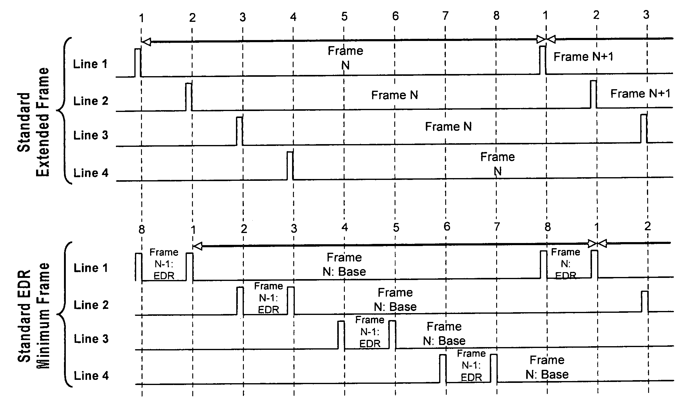
[0038]In general, the present invention is a self-contained CMOS imaging System-on-Chip whose dynamic range actively extends beyond the typical practical limit for imaging sensors set by the ratio of the maximum instantaneous linear signal swing (supported by the end-to-end signal path) to the minimum aggregate sensor noise (quadrature sum of all noise sources: pixel+analog signal chain+digitizer). Depending on exposure setup, dynamic range is enriched from the standard value by up to a maximum of 20×log(2N) dB where N is the number of A / D converter bits. In pr...


PUM


Abstract

A method and apparatus for an electronic image sensor having a base exposure, followed by a second or multiple exposures that are formed during signal readout. A timing controller controls the signal readout, such that as each line is read, the second and subsequent exposures are subsequently added to the base exposure to enrich the dynamic range. The image sensor may further include an analog-to-digital converter and noise suppression to further enhance the efficacy of the dynamic range enrichment. The system may also include additional signal processing and scaling functions.

Description

BACKGROUND OF THE INVENTION[0001]1. Field of the Invention[0002]The present invention relates generally to imaging sensors, and more particularly to an imaging system-on-chip solution for enhancing and controlling dynamic range, while maintaining high sensor performance.[0003]2. Description of the Related Art[0004]Visible imaging systems implemented using CMOS imaging sensors significantly reduce camera cost and power while improving resolution and reducing noise. The latest cameras use CMOS imaging System-on-Chip (iSoC) sensors that efficiently marry highly competitive image sensing with ancillary components including timing controller, clock drivers, reference voltages, A / D conversion and key signal processing elements. High-performance video cameras can hence be constructed using a single CMOS integrated circuit supported by only a lens and battery. These improvements translate into smaller camera size, longer battery life, and applicability to new cameras that simultaneously sup...

Claims


Application Information

Patent Timeline
Patent Type & Authority Patents(United States)
IPC IPC(8): H04N3/14H04N5/335H04N5/347H04N5/353H04N5/355H04N5/374H04N5/378
CPCH04N3/155H04N5/35581H04N5/2355H04N5/235H04N23/70H04N23/741H04N25/531H04N25/589
Inventor KOZLOWSKI, LESTER J.
Owner SAMSUNG ELECTRONICS CO LTD
Why Eureka
Try Eureka