
IC chip at-functional-speed testing with process coverage evaluation

a technology of process coverage and at-functional-speed testing, which is applied in the direction of stochastic cad, semiconductor/solid-state device testing/measurement, instruments, etc., can solve the problems of not determining the quality of at-functional-speed tests, functionality is not available in the prior, and current approaches do not correlate manufacturing testing, so as to improve process coverage of robust paths

Active Publication Date: 2009-11-17
SIEMENS PROD LIFECYCLE MANAGEMENT SOFTWARE INC
View PDF20 Cites 32 Cited by
  • Summary
  • Abstract
  • Description
  • Claims
  • Application Information

AI Technical Summary

Benefits of technology

The patent describes a method, system, and computer-readable medium for evaluating an integrated circuit (IC) chip. The method involves running a statistical static timing analysis (SSTA) of a full IC chip design, creating at-functional-speed test (AFST) robust paths for the chip, re-running the SSTA with a delay model setup based on the robust paths, calculating process coverage from the SSTA runnings, and evaluating the chip based on the process coverage. The technical effects of this patent include improved accuracy and efficiency in evaluating IC chips, as well as a more comprehensive coverage of process variations.

Problems solved by technology

One challenge relative to at-functional-speed testing is that IC chips tested represent, or include, only a small sampling of the overall fabrication process and operation condition variations the IC chip might see.
However, this functionality is not available in the prior art.
However, none of the current approaches identifies the amount of variation covered by a set of at-functional-speed test patterns, nor do they determine the quality of the at-functional-speed tests from a process coverage standpoint.
In addition, current approaches do not correlate manufacturing testing results with timing model accuracy based on changes in voltage, frequency or temperature, or based on process variations.

Method used


Image

  • IC chip at-functional-speed testing with process coverage evaluation
  • IC chip at-functional-speed testing with process coverage evaluation
  • IC chip at-functional-speed testing with process coverage evaluation

Examples


Embodiment Construction

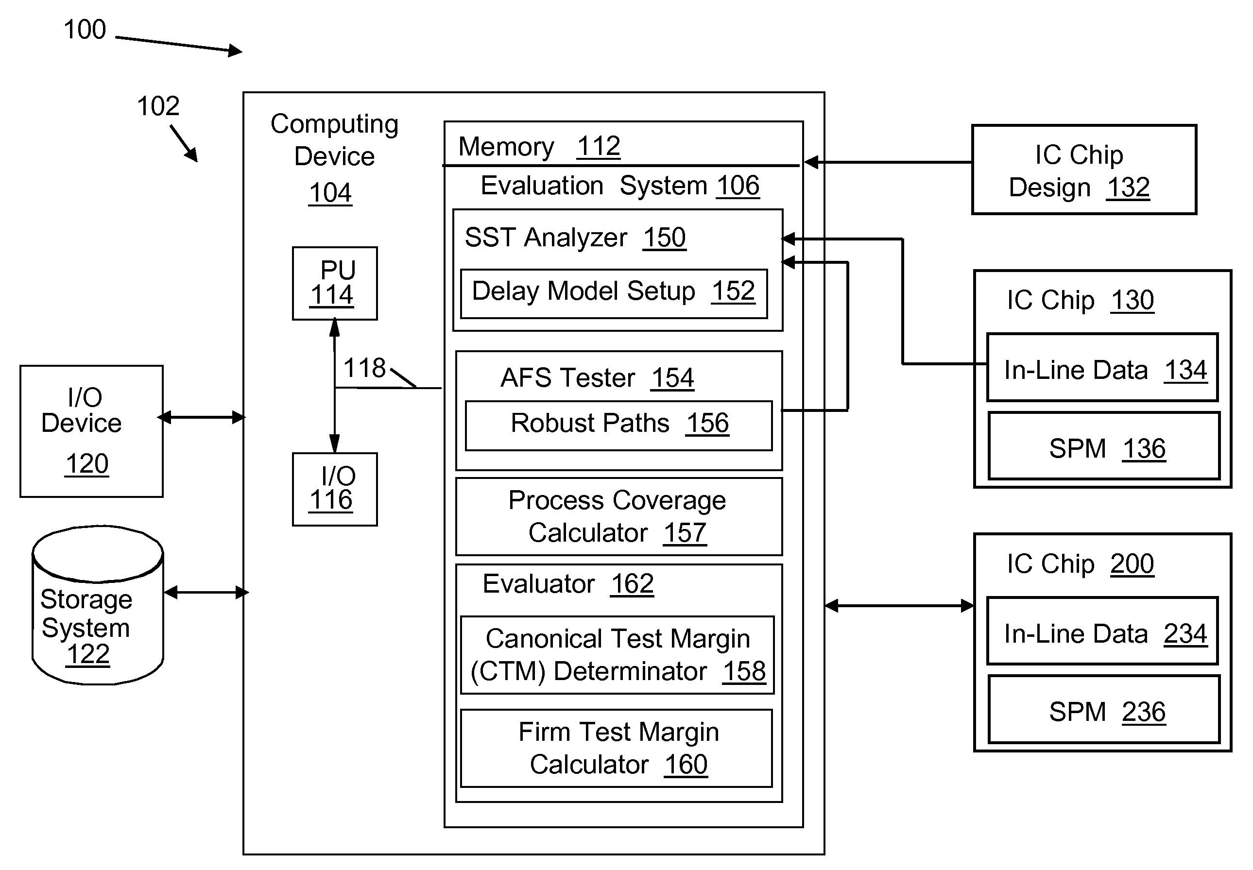
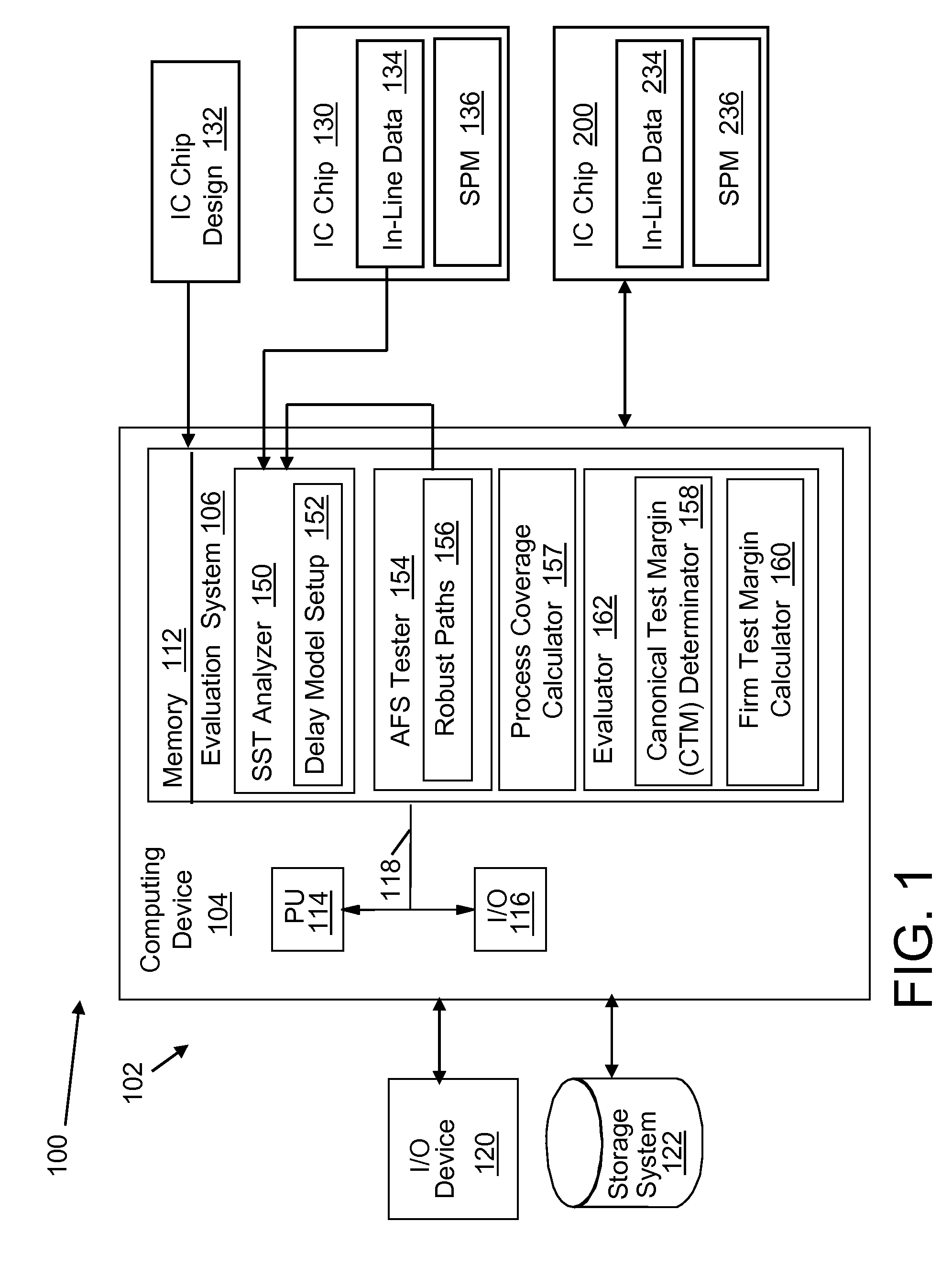
[0023]Turning to the drawings, FIG. 1 shows an illustrative environment 100 for evaluating an integrated circuit (IC) chip 130. To this extent, environment 100 includes a computer infrastructure 102 that can perform the various process steps described herein for evaluating an IC chip. In particular, computer infrastructure 102 is shown including a computing device 104 that comprises an evaluation system 106, which enables computing device 104 to evaluate an IC chip by performing the process steps of the disclosure.

[0024]As shown, an IC chip design 132 is provided to evaluation system 106 for statistical evaluation. IC chip design 132 can be used to model how an IC chip 130 generated based on IC chip design 132 may perform. After fabrication, an actual IC chip 130 including in-line data 134 is evaluated by evaluation system 106. In-line data 134 may include process conditions under which IC chip 130 was manufactured (in a certain time frame) and measured performance data of IC chip 1...


PUM


Abstract

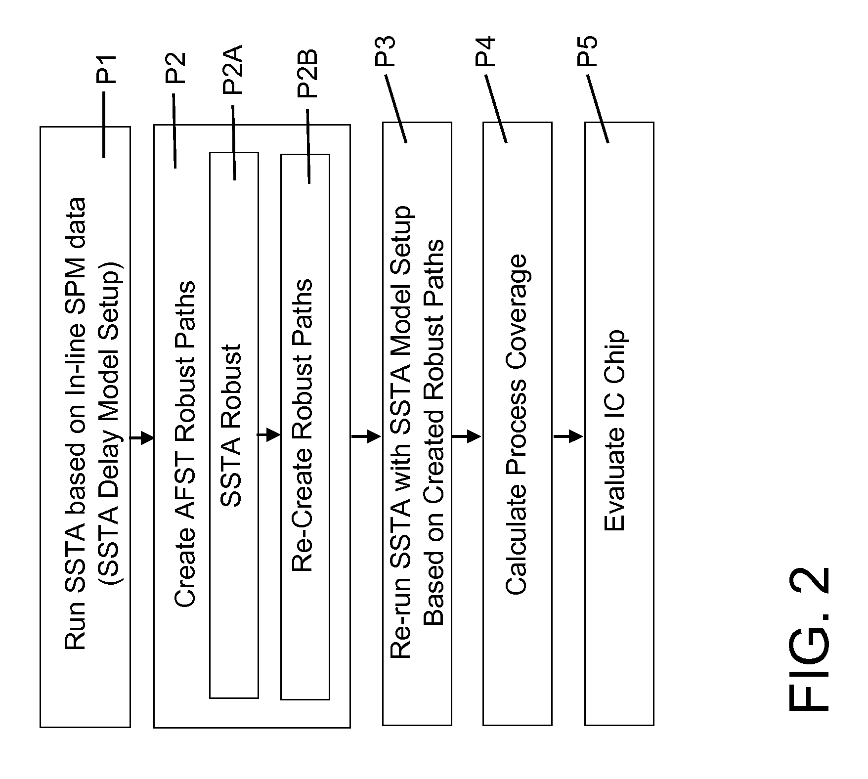
Methods, systems and program products for evaluating an IC chip are disclosed. In one embodiment, the method includes running a statistical static timing analysis (SSTA) of a full IC chip design; creating at-functional-speed test (AFST) robust paths for an IC chip, the created robust paths representing a non-comprehensive list of AFST robust paths for the IC chip; and re-running the SSTA with the SSTA delay model setup based on the created robust paths. A process coverage is calculated for evaluation from the SSTA runnings; and a particular IC chip is evaluated based on the process coverage.

Description

BACKGROUND[0001]1. Technical Field[0002]The disclosure relates generally to integrated circuit (IC) chip evaluation, and more particularly, to IC chip evaluation using at-functional-speed testing with process coverage evaluation.[0003]2. Background Art[0004]At-functional-speed testing of integrated circuit (IC) chips is frequently used to verify the functionality and performance of product IC chips. During IC chip fabrication, process variations may alter how an IC chip functions and / or performs. Further, fabrication process parameters can vary drastically from one IC chip fabrication lot to another, and within a lot. In addition, operating conditions within an IC chip vary during operation. One challenge relative to at-functional-speed testing is that IC chips tested represent, or include, only a small sampling of the overall fabrication process and operation condition variations the IC chip might see. However, it is important for IC chip fabricators to understand performance of fu...

Claims


Application Information

Patent Timeline
Patent Type & Authority Patents(United States)
IPC IPC(8): G06F17/50
CPCG06F17/5031G06F2217/10G06F30/3312G06F2111/08G01R31/3181G01R31/26H01L22/00
Inventor FOREMAN, ERIC A.GRISE, GARY D.HABITZ, PETER A.IYENGAR, VIKRAMLACKEY, DAVID E.VISWESWARIAH, CHANDRAMOULIXIONG, JINJUNZOLOTOV, VLADIMIR
Owner SIEMENS PROD LIFECYCLE MANAGEMENT SOFTWARE INC
Learn More