Switching device

a switching device and electric charge technology, applied in non-linear optics, instruments, nanoinformatics, etc., can solve the problems of insufficient reproducibility of switching devices using electric charge transfer complexes, difficult control of compositions, and difficulty in controlling compositions, so as to facilitate the operation, enhance the transfer probability, and stabilize the switching characteristics

Inactive Publication Date: 2009-11-24
FUJI ELECTRIC CO LTD
View PDF13 Cites 0 Cited by
  • Summary
  • Abstract
  • Description
  • Claims
  • Application Information

AI Technical Summary

Benefits of technology

[0009]The switching device according to the present invention is a switching device in which an organic bistable material layer containing an organic bistable compound having two types of stable resistance against an applied voltage is provided between at least two electrodes and is characterized in that a first electrode layer, an electric charge injection suppressing layer, an organic bistable material layer and a second electrode layer are sequentially formed to be respective thin films and, then, the electric charge injection suppressing layer comprises an electrically conductive layer which allows an electric charge injection amount from the first electrode layer to the organic bistable material layer to be small compared with that in a case in which the electric charge is directly injected from the first electrode layer to the organic bistable material layer without providing the electric charge injection suppressing layer.
[0010]Another aspect according to the present invention is a switching device in which an organic bistable material layer containing an organic bistable compound having two types of stable resistance against an applied voltage is provided between at least two electrodes and is characterized in that a second electrode layer, an organic bistable material layer, an electric charge injection suppressing layer and a first electrode layer are sequentially formed to be respective thin films and, then, the electric charge injection suppressing layer contains an electrically conductive layer which allows an electric charge injection amount from the first electrode layer to the organic bistable material layer to be small compared with that in a case in which the electric charge is directly injected from the first electrode layer to the organic bistable material layer without providing the electric charge injection suppressing layer.

Problems solved by technology

However, a switching device using the electric charge transfer complex has several problems.
First of all, since the electric charge transfer complex is constituted of an electron-donating molecule and an electron-accepting molecule at a rate of 1:1 by using a co-deposition method or the like, it has a shortcoming such that it is difficult to control a composition thereof.
Further, the switching device using the electric charge transfer complex has not sufficient reproducibility in the switching phenomenon and all devices produced in a same production condition do not necessarily exhibit switching characteristics.
Namely, there is a problem such that appearance probability of devices which perform switching (transfer) is low.
Further, even when the transfer is noticed, there is a problem such that, particularly, a transfer voltage from the off state to the on state is not constant.

Method used


Image

  • Switching device
  • Switching device
  • Switching device

Examples


example 1

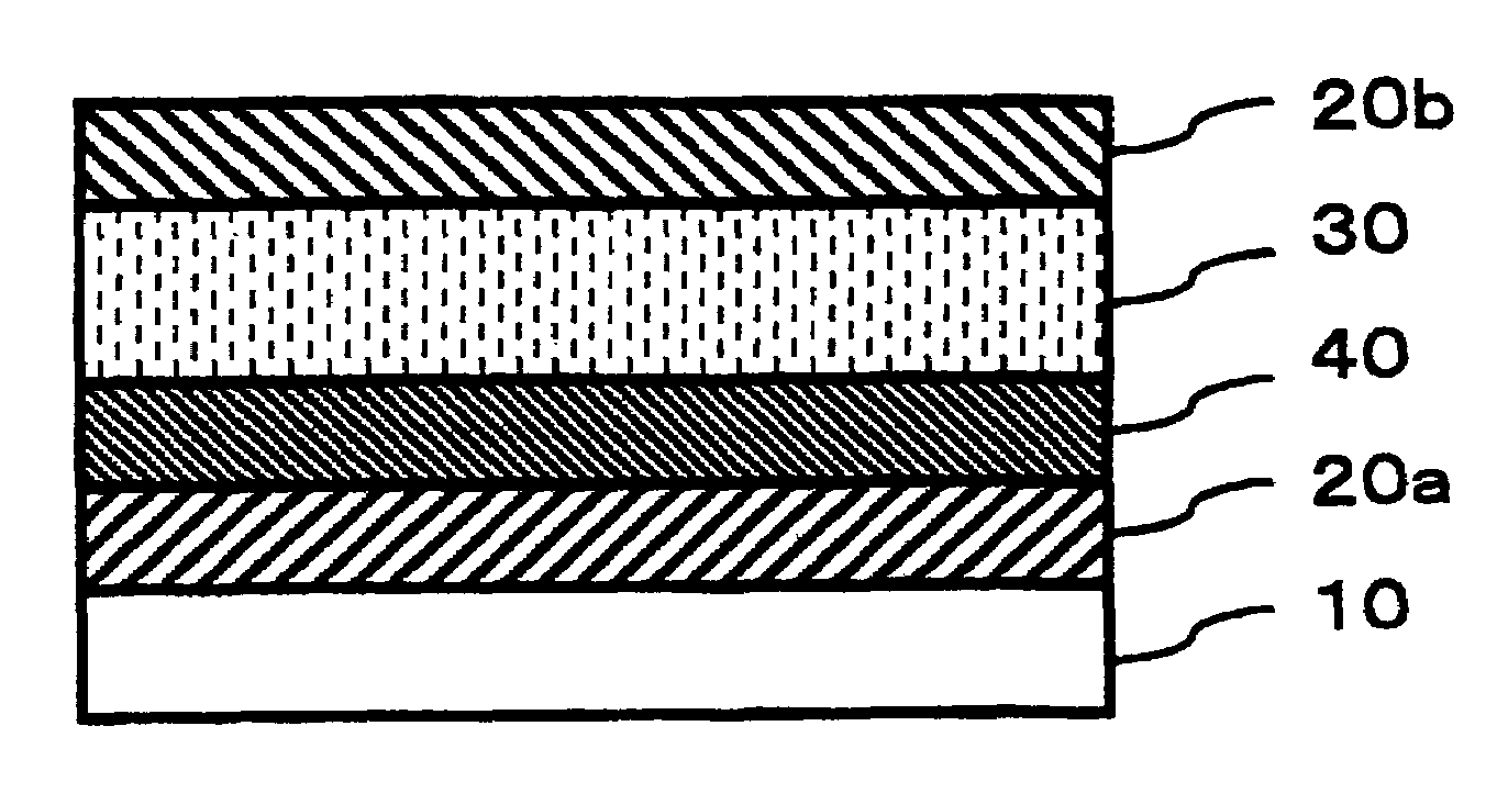
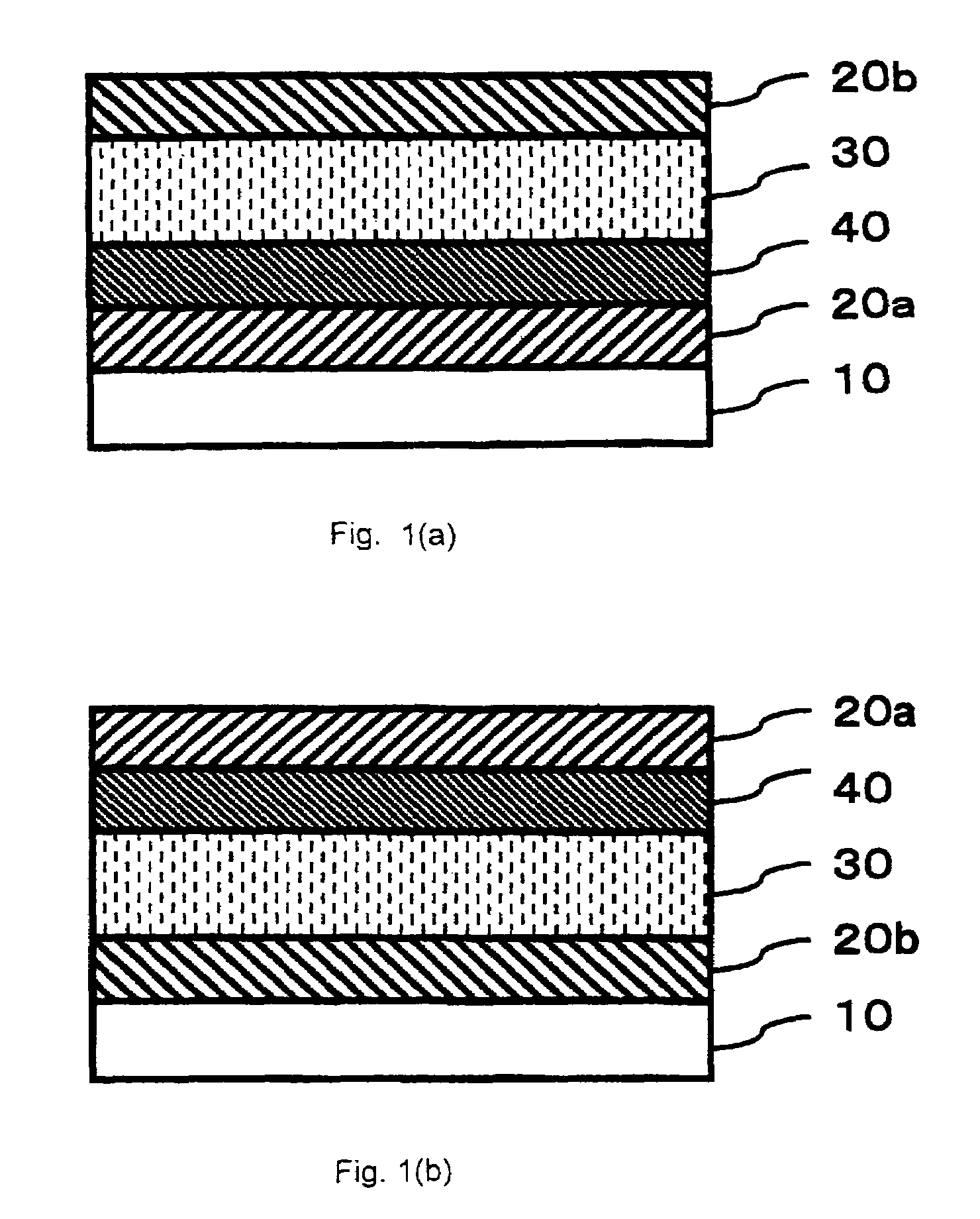
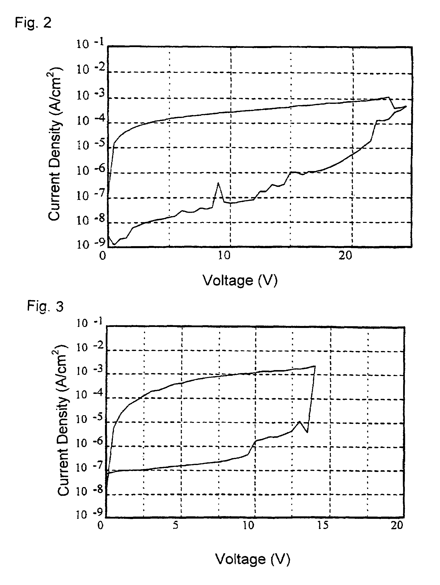
[0088]In accordance with procedures to be described below, a switching device having a constitution as shown in FIG. 1a was prepared. Namely, while using a glass substrate as a substrate 10, a first electrode layer 20a, an electric charge injection suppressing layer 40, an organic bistable material layer 30, and a second electrode layer 20b are sequentially formed to be respective thin films by a vacuum deposition method in the stated order such that they came to be 100 nm, 10 nm, 60 nm and 100 nm, respectively, to thereby form the switching device according to Example 1.

[0089]As for a deposition source, namely, raw material, of each layer, aluminum is used as the first electrode layer 20a, gold is used as the second electrode layer 20b, and a quinomethane compound represented by the above-described formula (I-1) is used as the organic bistable material layer 30. Further, the electric charge injection suppressing layer 40 was formed by subjecting aluminum to reactive deposition in a...

example 2

[0090]A switching device according to Example 2 was obtained in a same condition as in Example 1, except that a thickness of the electric charge injection suppressing layer 40 was set to be 20 nm and a thickness of the organic bistable material layer 30 was set to be 80 nm.

example 3

[0091]A switching device according to Example 3 was obtained in a same condition as in Example 1, except that an oxygen partial pressure at the time of forming the electric charge injection suppressing layer 40 was set to be 1×10⁻⁵ torr.


PUM

PropertyMeasurementUnit
volume resistivityaaaaaaaaaa
thicknessaaaaaaaaaa
temperatureaaaaaaaaaa

Abstract

A switching device in which an organic bistable material layer containing an organic bistable compound having two types of stable resistance against an applied voltage is provided between at least two electrodes. In the switching device, a first electrode layer, an electric charge injection suppressing layer, an organic bistable material layer and a second electrode layer are sequentially formed on a substrate as respective thin films, in which the electric charge injection suppressing layer contains an electrically conductive layer which allows an electric charge injection amount from the first electrode layer to the organic bistable material layer to be small compared with that in a case in which the electric charge is directly injected from the first electrode layer to the organic bistable material layer without providing the electric charge injection suppressing layer.

Description

BACKGROUND[0001]The present invention relates to a switching device for driving of a display panel which uses an organic EL, a liquid crystal or the like, or a switching device to be utilized in a high density memory or the like.[0002]In recent years, the characteristics of an organic electronic material have remarkably been improved. Particularly, it has been considered as to whether a so-called organic bistable material in which, when a voltage is continuously applied on the material in an increasing manner, a current in a circuit is abruptly increased at a given voltage or more and a switching phenomenon is observed can be applied to a switching device for driving an organic EL display panel, a high density memory, or the like.[0003]In FIG. 11, an example of voltage-current characteristics of an organic bistable material which shows such switching behavior as described above is shown. As shown in FIG. 11, the organic bistable material has two types of current-voltage characterist...

Claims


Application Information

Patent Timeline
Patent Type & Authority Patents(United States)
IPC IPC(8): C09K19/02G02F1/1343H01L51/00H01L27/10H01L51/30
CPCB82Y10/00H01L51/0052H01L51/0067H01L51/0068H01L51/0591H01L51/0065H01L51/0051H01L51/0059H01L51/0595H01L51/0081H10K85/611H10K85/653H10K85/655H10K85/615H10K85/631H10K85/654H10K85/324H10K10/50H10K10/701H10K85/649H10K30/671H10K10/20
Inventor KAWAKAMI, HARUOKATO, HISATOYAMASHIRO, KEISUKEKATO, KYOKO
Owner FUJI ELECTRIC CO LTD
Why Eureka
Try Eureka