Nonvolatile semiconductor memory for storing multivalued data

a nonvolatile semiconductor and data storage technology, applied in static storage, digital storage, instruments, etc., can solve the problem that the address space of nonvolatile semiconductor memory cannot be used efficiently, and achieve the effect of increasing the speed of the operation

Active Publication Date: 2009-11-24
CETUS TECH INC
View PDF14 Cites 20 Cited by
  • Summary
  • Abstract
  • Description
  • Claims
  • Application Information

AI Technical Summary

Benefits of technology

[0048]According to the invention, it is possible to provide a nonvolatile semiconductor memory for storing multivalued dat

Problems solved by technology

Referring to the operation for dropping the threshold voltage of the memory cell, however, a flash memory is only permitted to carry out an erasing operation for collectively dropping a threshold voltage on a unit of a block in respect of a

Method used


Image

  • Nonvolatile semiconductor memory for storing multivalued data
  • Nonvolatile semiconductor memory for storing multivalued data
  • Nonvolatile semiconductor memory for storing multivalued data

Examples


first embodiment

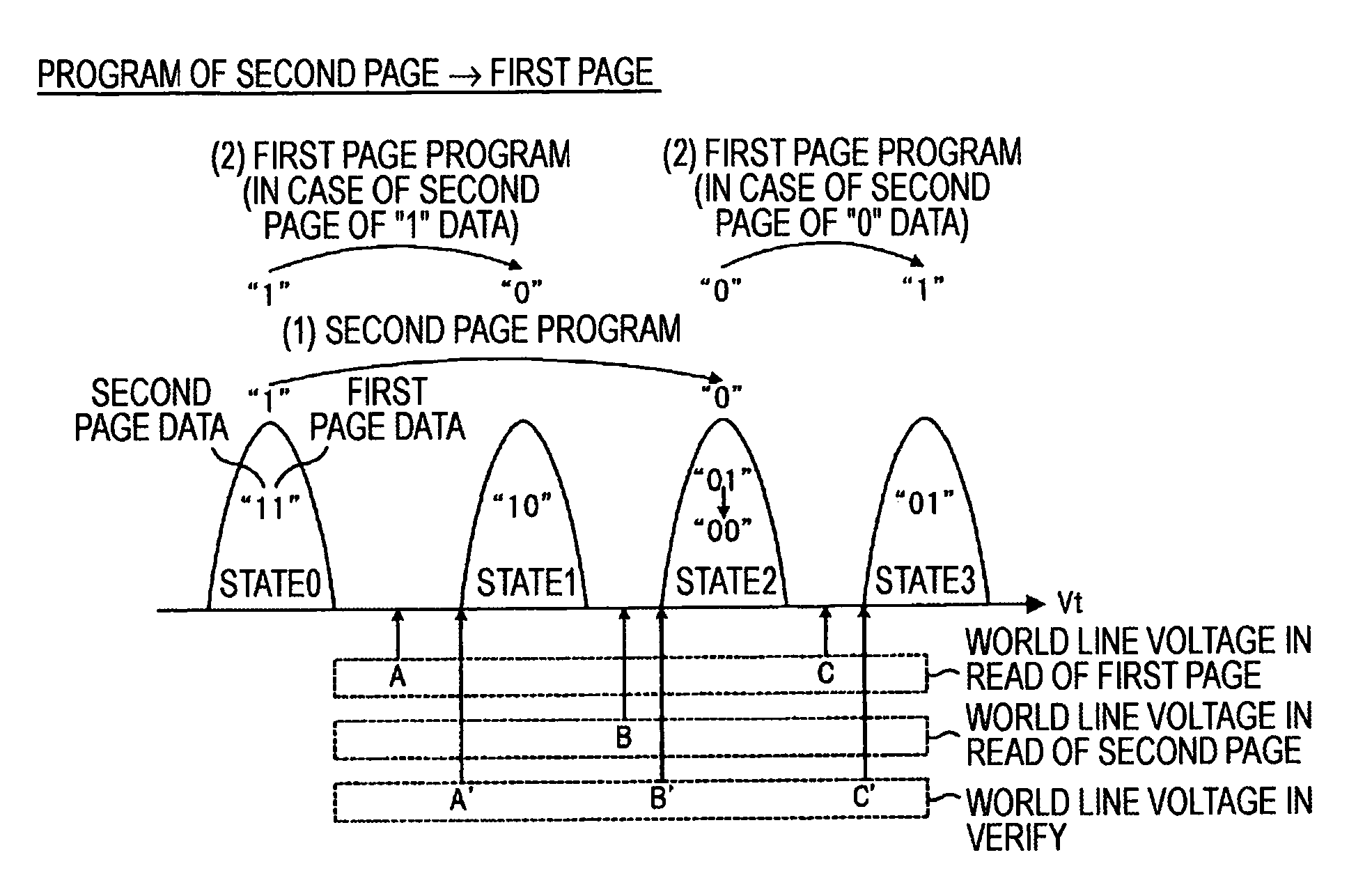
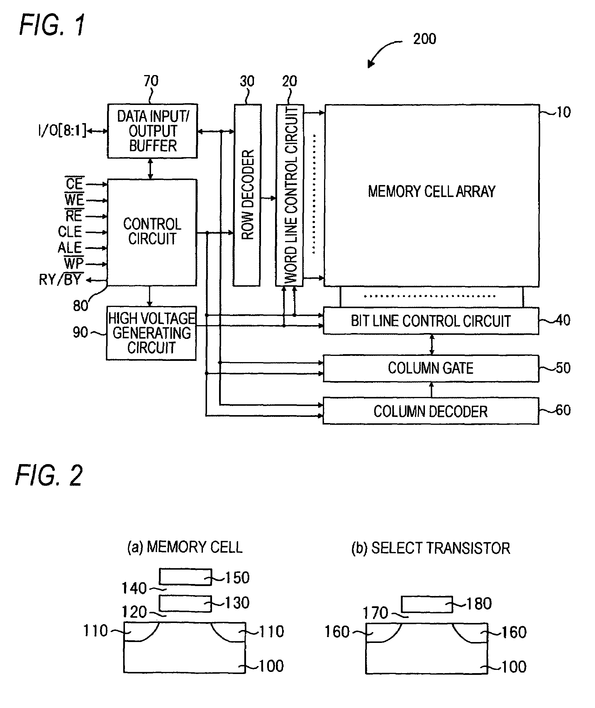
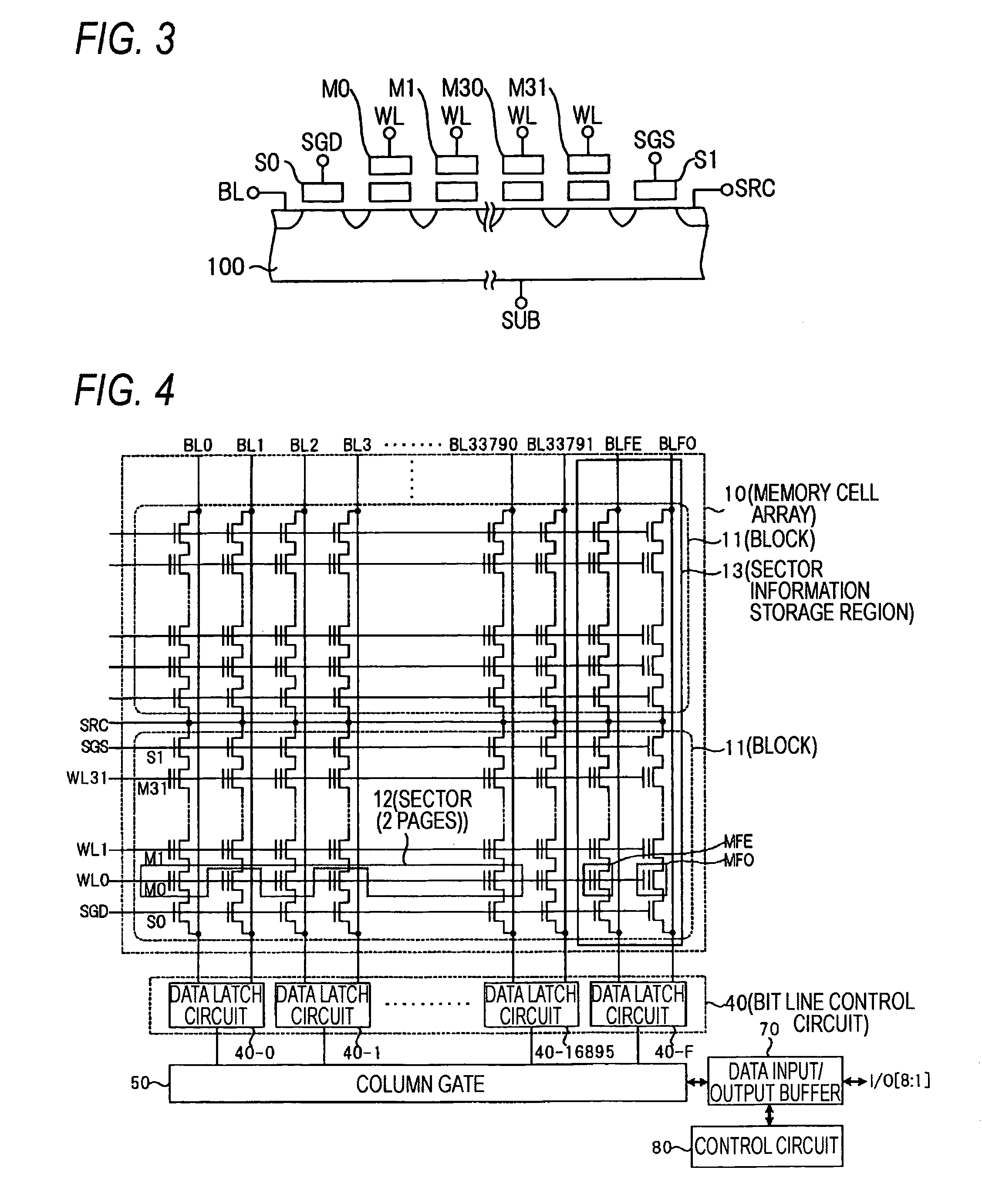
[0063]FIG. 1 is a diagram showing a schematic structure of a nonvolatile semiconductor memory 200 according to a first embodiment. In FIG. 1, a memory cell array 10 includes a plurality of word lines and a plurality of bit lines, and memory cells are disposed in a matrix on intersecting points of the word lines and the bit lines. A word line control circuit 20 and a bit line control circuit 40 are connected to the memory cell array 10.

[0064]The word line control circuit 20 serves to select a predetermined word line in the memory cell array 10 and to apply necessary voltages for read, write (programming) and erase. A row decoder 30 serves to control the word line control circuit 20, thereby selecting a predetermined word line.

[0065]The bit line control circuit 40 includes a plurality of data latch circuits as will be described below, and serves to read data of the memory cell in the memory cell array 10 through the bit line, to detect (verify) the state of the memory cell in the memo...

second embodiment

[0129]Next, a second embodiment according to the invention will be described with reference to the drawings.

[0130]FIG. 11 is a diagram showing a structure of a nonvolatile semiconductor memory 200 according to the second embodiment. In FIG. 11, components having the same functions as those in the first embodiment have the same reference numerals and detailed description thereof will be omitted. Only portions having different structures will be described below.

[0131]FIG. 11 is different from FIG. 4 described in the first embodiment in that a sector information storage region has a different structure. While the sector information storage region 13 is disposed in the memory cell array 10 in the first embodiment, the sector information storage region is comprised of a ferroelectric memory (FeRAM) 300 in the second embodiment.

[0132]Thus, the sector information storage region is comprised of the ferroelectric memory (FeRAM) 300 capable of carrying out a high-speed reading operation, a hi...


PUM


Abstract

A nonvolatile semiconductor memory according to the invention includes a memory cell array comprised of a multivalued memory cell for storing data on a plurality of pages, a data processing circuit for carrying out a read operation for reading data from the memory cell array and a programming operation for writing the data to the memory cell array on a page unit, and a control circuit for controlling an operation of the data processing circuit, the control circuit changing an assignment of data corresponding to a threshold voltage distribution of the multivalued memory cell depending on order of a page over which the programming operation is to be carried out in such a manner that the programming operation is executed by a transition of a threshold voltage of the multivalued memory cell in a positive direction.

Description

BACKGROUND OF THE INVENTION[0001]1. Field of the Invention[0002]The present invention relates to a nonvolatile semiconductor memory for storing multivalued data by an electrical rewrite.[0003]2. Description of the Related Art[0004]In recent years, a nonvolatile semiconductor memory, particularly, a flash memory can electrically rewrite data and can hold the data also in a state in which a power supply is turned OFF. Therefore, a large number of nonvolatile semiconductor memories have been used as memories for data storage of portable apparatuses such as a cell phone, a digital camera and a silicon audio player.[0005]These portable apparatuses deal with images, animations and music data having a large data volume. In the nonvolatile semiconductor memory, therefore, it has been further demanded to implement an increase in a capacity and a reduction in a cost. Examples of a nonvolatile semiconductor memory capable of implementing the increase in a capacity and the reduction in a cost i...

Claims


Application Information

Patent Timeline
IPC IPC(8): G11C16/04
CPCG11C11/5628G11C11/5642G11C16/10G11C16/3459G11C16/0483G11C2211/5621
Inventor KOUNO, KAZUYUKI
Owner CETUS TECH INC
Why Eureka
Try Eureka