Electromagnetic wave shield case and a method for manufacturing electromagnetic wave shield case

a technology of electromagnetic shield and shield case, which is applied in the direction of magnetic materials, electrical equipment, magnetic bodies, etc., can solve the problems of high manufacturing cost, limited space, and thick circuit board, and achieve the effect of convenient molding of shield cas

Inactive Publication Date: 2009-12-01
NGK INSULATORS LTD +1
View PDF29 Cites 31 Cited by
  • Summary
  • Abstract
  • Description
  • Claims
  • Application Information

AI Technical Summary

Benefits of technology

[0017]However, Prior Art #1 has a problem in that the height of the shield case 50B is apt to be high, and a reduction in the thickness of the circuit board 1 is disturbed, resulting in a high cost of manufacturing.
[0027]In order to achieve the objective, a first aspect of the present invention is an electromagnetic wave shield case comprising a shield case body configured to cover electronic parts on a circuit board, and a flange formed integrally with said shield case body, wherein said shield case body and said flange are made of metallic material having a value of about 0.01 or more expressed by a fracture strength / elastic constant, and said flange is elastically deformed to be grounded to an grounding conduction portion on said circuit board to prevent a leakage of electromagnetic waves to outside of said electromagnetic wave shield case.
[0033]A fifth aspect of the present invention is an electromagnetic wave shield case comprising a shield case body configured to cover electronic parts on a circuit board, and a flange formed integrally with said shield case body, wherein, said shield case body and said flange are made of metallic glass, and said flange is elastically deformed to be grounded to an grounding conduction portion on said circuit board to prevent a leakage of electromagnetic waves to outside of said electromagnetic wave shield case.
[0034]According to the fifth aspect of the present invention, since the electromagnetic wave shield case is manufactured using metallic glass, it is possible to utilize a deformation due to viscous flowing on the atomic level which is different from a plastic deformation, and thus a high precision flange can be formed without a spring-back.
[0043]Thus, it is possible to easily mold the shield case and the like, which has a dome shape, other shapes including a nonsymmetrical shape, or which has a flange having an external periphery portion with non-straight lines.

Problems solved by technology

However, Prior Art #1 has a problem in that the height of the shield case 50B is apt to be high, and a reduction in the thickness of the circuit board 1 is disturbed, resulting in a high cost of manufacturing.
In cellular phones and computers in which the thickness has become rapidly thinner, limitations with respect to their spaces are brought due to the layout of electronic parts.
Therefore, provisioning of the number of through holes, which is necessary and sufficient, on a circuit board has come to be no longer permitted, and a new problem in that Prior Art #2, cannot be applied is occurring.
Although Prior Art #3 does not require provision of a through hole in a circuit board, Prior Art #3 has the following new problem regarding realization of a reliable electric connection of the shield case and the metallic ground line.

Method used


Image

  • Electromagnetic wave shield case and a method for manufacturing electromagnetic wave shield case
  • Electromagnetic wave shield case and a method for manufacturing electromagnetic wave shield case
  • Electromagnetic wave shield case and a method for manufacturing electromagnetic wave shield case

Examples


Embodiment Construction

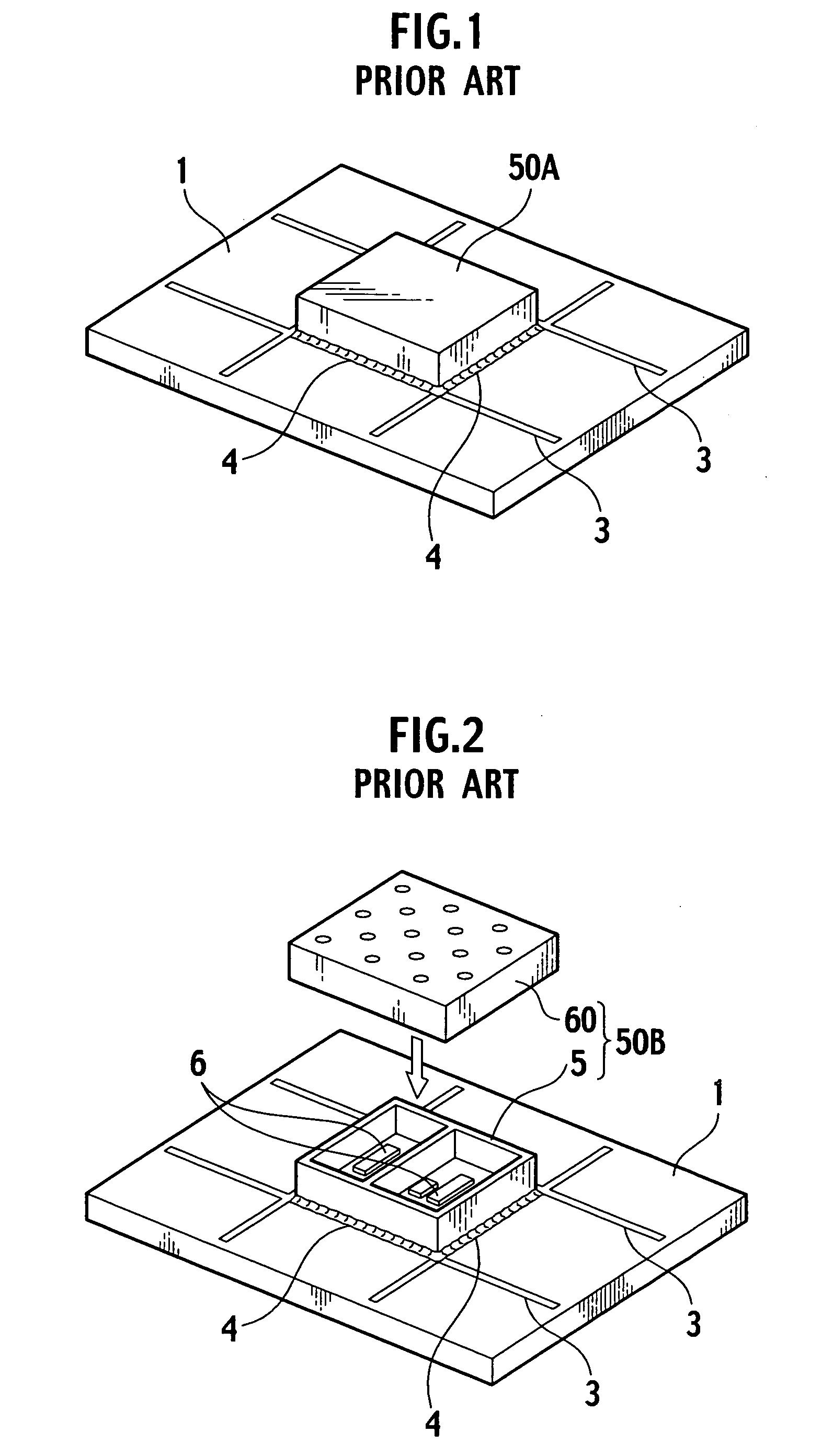
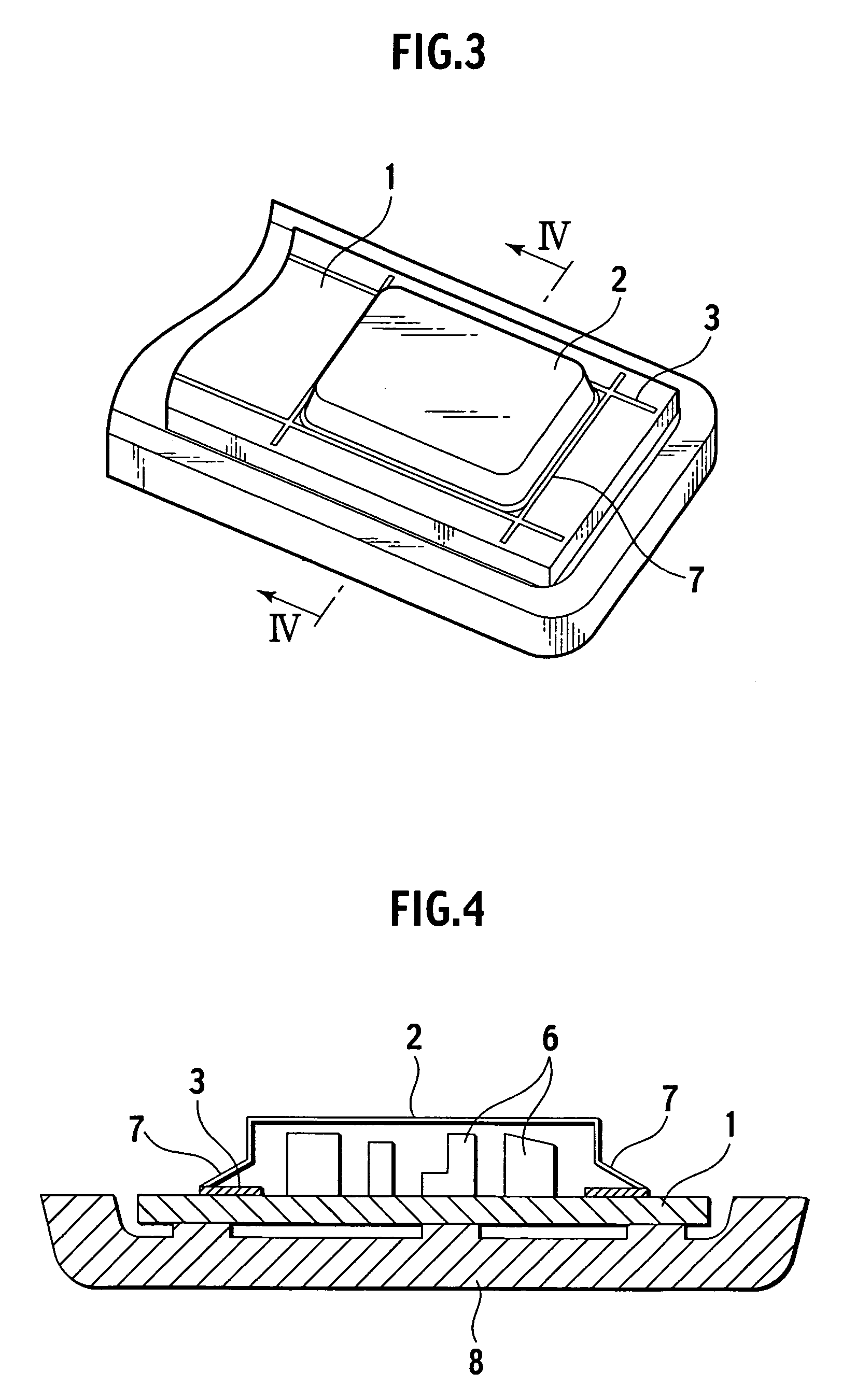
[0064]Embodiments of the present invention will be described below. Note that the same components as those in FIGS. 1 and 2 are denoted by the same reference numeral and symbols, and descriptions for them are omitted.

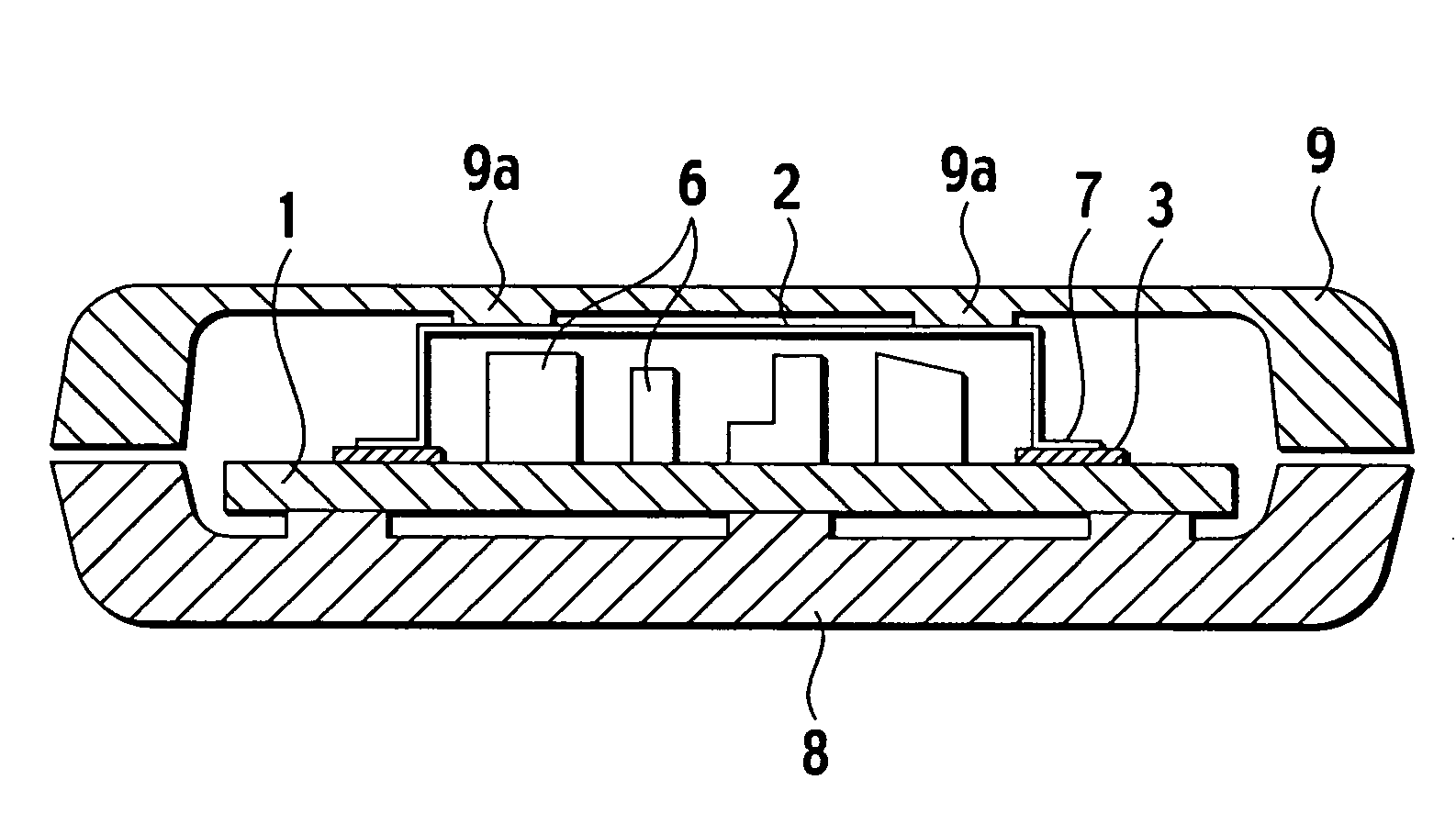
[0065]FIGS. 3 and 4 show a shield case 2 shielding electromagnetic wave according to an embodiment of the present invention. The shield case 2 is disposed to cover electronic parts 6 on a circuit board 1. A flange 7 formed integrally with the shield case 2 (shield case body), which is elastically deformed to be grounded to a metallic ground line 3 (grounding conduction portion) on the circuit board 1, so that leakage of electromagnetic waves to the outside of the shield case 2 is prevented.

[0066]The flange 7 is manufactured integrally with the shield case 2. The shield case 2 and the flange 7 are made of metallic material having a value (ratio) of about 0.01 or more (not less than 0.01) expressed by a fracture strength(σf) / elastic constant(E).

[0067]Further, in this embo...


PUM

PropertyMeasurementUnit
angleaaaaaaaaaa
widthaaaaaaaaaa
thicknessaaaaaaaaaa

Abstract

An objective of the present invention is to form a hyper-elastic flange integrally within a shield case body around a periphery thereof while decreasing an occupied area for grounding. The shield case 2 according to the present invention is disposed to cover electronic parts 6 on a circuit board 1, and which has a flange 7 formed integrally therewith so as to contact with a metallic ground line 3 on the circuit board 1. The flange 7 is elastically deformed to be grounded, thus a leakage of electromagnetic waves to the outside of the shield case 2 is prevented. The flange 7 is made of metallic glass. By forming the flange 7 from metallic glass, a displacement due to viscous flowing on the atomic level, which is different from a plastic deformation, can be utilized, and thus a high precision flange can be formed without a spring-back.

Description

CROSS REFERENCE TO RELATED APPLICATIONS[0001]This application is based upon and claims the benefit of priority from the prior Japanese Patent Applications No. P2004-2995, filed on Jan. 8, 2004; the entire contents of which are incorporated herein by reference.BACKGROUND OF THE INVENTION[0002]1. Field of the Invention[0003]The present invention relates to an electromagnetic wave shield case disposed to cover electronic parts on a circuit board (printed circuit board) used for a cellular phone and a computer, and an electromagnetic wave shield case manufacturing method.[0004]2. Description of the Related Art[0005]When electronic parts such as an oscillator for generating electromagnetic waves are present on a circuit board, preventing influence on other circuit devices due to electromagnetic waves is required.[0006]Specifically, in order to prevent occurrence of radiation noise, technologies have been identified that shielding the electronic parts so as not to propagate generated elec...

Claims


Application Information

Patent Timeline
Patent Type & Authority Patents(United States)
IPC IPC(8): H05K9/00H01F1/153
CPCH05K9/0069H05K9/0026H01F1/15358H05K9/00
Inventor MURAMATSU, NAOKUNIINOUE, AKIHISAZHANG, TAOKIMURA, HISAMICHI
Owner NGK INSULATORS LTD
Why Eureka
Try Eureka