
Vertical spin transistor and method of manufacturing the same

a technology of vertical spin transistor and manufacturing method, which is applied in the direction of electrical equipment, semiconductor devices, magnetic bodies, etc., can solve the problems of difficult formation of source and drain sections, difficult manufacturing of spin transistors,

Inactive Publication Date: 2009-12-08
KK TOSHIBA
View PDF6 Cites 18 Cited by
  • Summary
  • Abstract
  • Description
  • Claims
  • Application Information

AI Technical Summary

Benefits of technology

This design simplifies the manufacturing process of spin transistors, reduces manufacturing difficulties, and allows for a rewritable programmable integrated circuit with a short channel length exceeding lithography technique limits.

Problems solved by technology

However, there is a problem that it is difficult to manufacture the spin transistor.
In particular, difficulty in forming source and drain sections is often a problem.

Method used


Image

  • Vertical spin transistor and method of manufacturing the same
  • Vertical spin transistor and method of manufacturing the same
  • Vertical spin transistor and method of manufacturing the same

Examples


first embodiment

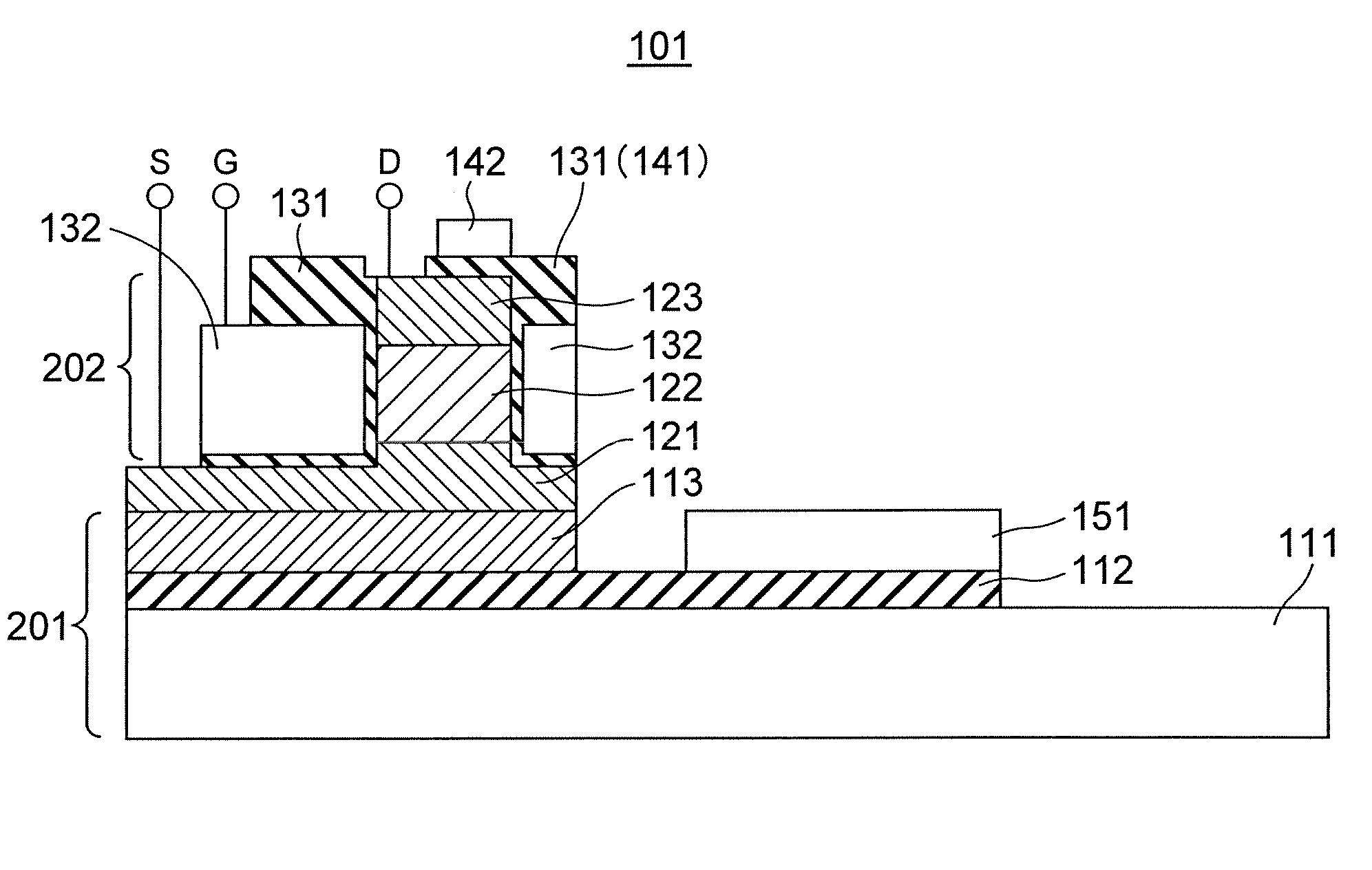
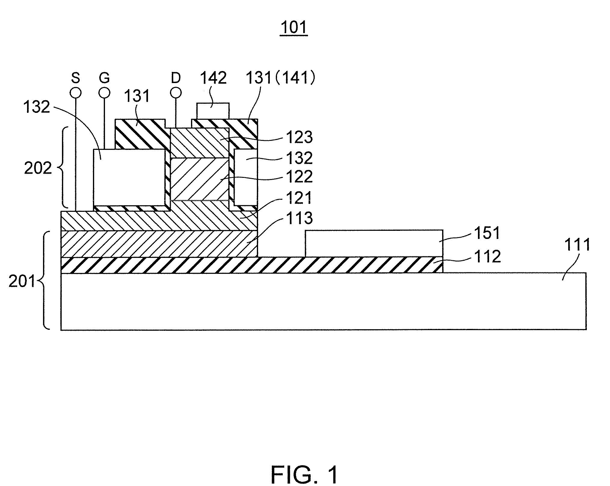
[0025]FIG. 1 is a side sectional view of a vertical spin transistor 101 according to a first embodiment of the present invention. A substrate 111, an insulating film 112, and a semiconductor layer 113 are present below the vertical spin transistor 101. The vertical spin transistor 101 includes a first source / drain layer 121, a channel layer 122, a second source / drain layer 123, a gate insulating film 131, a gate electrode 132, an insulating layer 141, and a spin writing line 142.

[0026]The substrate 111 is, here, a semiconductor substrate, specifically, a silicon substrate formed of silicon. The insulating film 112 is formed on the substrate 111. The insulating film 112 is, here, an embedded insulating film formed of insulator, specifically, an embedded silicon oxide film formed of silicon oxide. The semiconductor layer 113 is formed on the insulating film 112. The semiconductor layer 113 is, here, a Ge layer formed of Ge (germanium). The vertical spin transistor 101 is provided on a...

second embodiment

[0069]FIG. 8A is a side sectional view of the vertical spin transistor 101 according to the second embodiment. The substrate 111, the insulating film 112, and the semiconductor layer 113 are present below the vertical spin transistor 101 in FIG. 8A. The vertical spin transistor 101 in FIG. 8A includes the first source / drain layer 121, the channel layer 122, the second source / drain layer 123, the gate insulating film 131, the gate electrode 132, and a magnetic recording layer 161.

[0070]The vertical spin transistor 101 according to the second embodiment includes, instead of the spin writing line 142, the magnetic recording layer 161 including a magnetic layer. In the vertical spin transistor 101 according to the second embodiment, spin injection writing scheme is adopted instead of current control writing scheme.

[0071]The first source / drain layer 121 is formed on the semiconductor layer 113. The first source / drain layer 121 is, here, a magnetic layer formed of magnetic material, speci...

third embodiment

[0077]FIG. 8B is a side sectional view of the vertical spin transistor 101 according to the third embodiment. The substrate 111, the insulating film 112, and the semiconductor layer 113 are present below the vertical spin transistor 101 in FIG. 8B. The vertical spin transistor 101 in FIG. 8B includes the first source / drain layer 121, the channel layer 122, the second source / drain layer 123, the gate insulating film 131, the gate electrode 132, and a magnetic recording layer 161.

[0078]The vertical spin transistor 101 according to the third embodiment includes, instead of the spin writing line 142, the magnetic recording layer 161 including a magnetic layer. In the vertical spin transistor 101 according to the third embodiment, spin injection writing scheme is adopted instead of current control writing scheme.

[0079]The first source / drain layer 121 is formed on the semiconductor layer 113. The first source / drain layer 121 is, here, a two-layer film formed by sequentially stacking a mag...


PUM


Abstract

A vertical spin transistor according to an embodiment of the present invention includes: a first source / drain layer including a layer formed of magnetic material; a protruding structure including, a channel layer formed on the first source / drain layer and including a layer formed of semiconductor, and a second source / drain layer formed on the channel layer and including a layer formed of magnetic material; a gate insulating film formed on a side of the channel layer; and a gate electrode formed on a surface of the gate insulating film.

Description

CROSS REFERENCE TO RELATED APPLICATION[0001]This application is based upon and claims the benefit of priority from prior Japanese Patent Application No. 2007-58782, filed on Mar. 8, 2007, the entire contents of which are incorporated herein by reference.BACKGROUND OF THE INVENTION[0002]1. Field of the Invention[0003]The present invention relates to a vertical spin transistor and a method of manufacturing the same.[0004]2. Background Art[0005]Conventionally, increases in speed and improvements of performance of MOSFETs have been realized mainly by reducing the device size. However, in recent years, due to the limit in the lithography technique, various proposals concerning new channel materials and channel structures have been actively made. A representative example is a strain application technique for applying strain to Si crystals in a channel section. Besides, a method of using SiGe crystals or Ge crystals in a channel section of a p-type MOSFET is also reported. It is known that...

Claims


Application Information

Patent Timeline
Patent Type & Authority Patents(United States)
IPC IPC(8): H01L29/82
CPCH01F10/1936H01L29/42392H01L29/78642H01L29/7848H01L29/66984
Inventor SUGIYAMA, NAOHARUSAITO, YOSHIAKI
Owner KK TOSHIBA
Learn More