Supercharge Your Innovation With Domain-Expert AI Agents!

Liquid crystal display device and method of fabricating the same

a technology of liquid crystal display and display device, which is applied in the direction of semiconductor devices, instruments, optics, etc., can solve the problems of high minuteness of display device, complicated production process, and inability to achieve 1 cmsup>2/sup>/vsec of a-si tft,

Active Publication Date: 2009-12-15
LG DISPLAY CO LTD
View PDF3 Cites 1 Cited by
  • Summary
  • Abstract
  • Description
  • Claims
  • Application Information

AI Technical Summary

Benefits of technology

The present invention is about a new liquid crystal display device and a method of fabricating it. The invention aims to overcome the limitations and disadvantages of existing technology. The technical effects of the invention include the formation of active patterns in the pixel unit and circuit unit of a substrate, the formation of insulating films and gate electrodes, the exposure of source and drain regions through contact holes, the attachment of a second substrate, and the formation of a liquid crystal layer between the two substrates. These features improve the performance and reliability of the liquid crystal display device.

Problems solved by technology

However, electric mobility (˜1 cm2 / Vsec) of the a-Si TFT is not desired for a peripheral circuit requiring a high speed operation over 1 MHz.
Accordingly, the display device has high minuteness.
As compared with the a-Si TFT LCD device forming single type channels, the driving circuit-integrated LCD device complicates the production process.
As a result, the plurality of photolithography processes decrease the production yield and increase a probability of generating defects on the TFTs.
The mask that forms the patterns is very expensive.
If the number of the masks increases, the production cost of the LCD device increases.

Method used


Image

  • Liquid crystal display device and method of fabricating the same
  • Liquid crystal display device and method of fabricating the same
  • Liquid crystal display device and method of fabricating the same

Examples


second embodiment

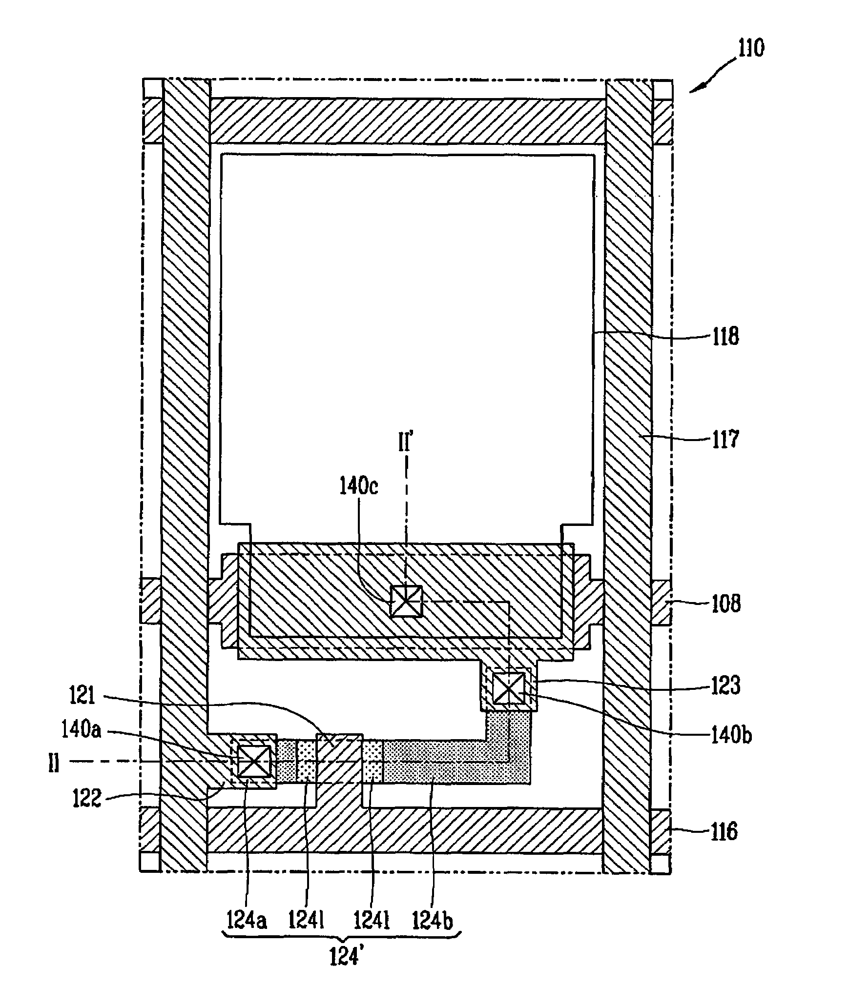
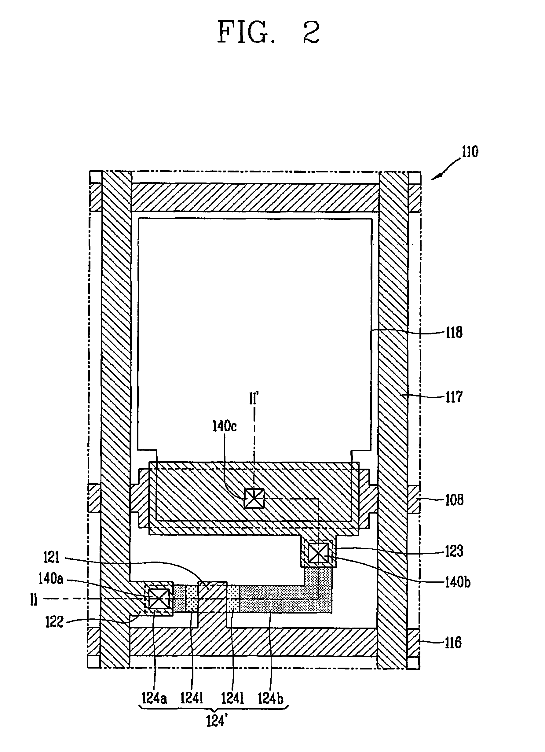
[0062]In the array substrate 210 of the second embodiment, the source / drain electrodes 222 and 223, the data line 217, the source / drain electrode patterns, the data line pattern and the pixel electrode 218 may be formed by a single mask process using diffraction (or half-tone) mask. The contact hole forming process for the pixel electrode 218 is not necessary. The array substrate 210 may be fabricated by the four mask processes, which will now be explained in detail with reference to the method of fabricating the LCD device.

[0063]FIGS. 5A to 5D are cross-sectional views illustrating sequential steps of a fabrication process of the array substrate, taken along line IV-IV′ of FIG. 4, and FIGS. 6A to 6D are plane views illustrating sequential steps of the fabrication process of the array substrate, taken along line IV-IV′ of FIG. 4.

[0064]The second exemplary embodiment illustrates a driving circuit-integrated LCD device including p channel TFTs in a pixel unit and a circuit unit.

[0065]...

third embodiment

[0095]In the array substrate 310 of the third embodiment, the source / drain electrodes 322 and 323, the data line 317, the source / drain electrode patterns, the data line pattern and the pixel electrode 318 may be formed by single mask process using diffraction mask. The contact hole forming process for the pixel electrode 318 is not necessary. As a result, the array substrate 310 may be fabricated by the four mask processes, which will now be explained in detail with reference to the method of fabricating the LCD device.

[0096]FIGS. 9A to 9D are cross-sectional views illustrating sequential steps of a fabrication process of the array substrate, taken along line VIII-VIII′ of FIG. 8, and FIGS. 10A to 10D are plane views illustrating sequential steps of the fabrication process of the array substrate, taken along line VIII-VIII′ of FIG. 8.

[0097]As shown in FIGS. 9A and 10A, a poly-Si thin film is formed by forming a buffer layer 311 and an a-Si thin film on a substrate 310 made of a tran...


PUM

PropertyMeasurementUnit
conductiveaaaaaaaaaa
photosensitiveaaaaaaaaaa
thicknessaaaaaaaaaa

Abstract

An LCD device and a method of fabricating the same are provided. The LCD device comprises a first substrate divided into a pixel unit and a circuit unit. Active patterns are disposed in the pixel unit and the circuit unit of the first substrate. A first insulating film is disposed on the first substrate. Gate electrodes are disposed in the pixel unit and the circuit unit of the first substrate, and common lines are disposed in the pixel unit of the first substrate. First contact holes and second contact holes are disposed in regions of the first insulating film, the first interlayer insulating film and the second interlayer insulating film. Source electrodes and drain electrodes electrically connect to the source regions and the drain regions of the active patterns through the first contact holes and the second contact holes.

Description

[0001]This patent document claims the benefit of Korean Patent Application 2006-61665 filed on Jun. 30, 2006, which is hereby incorporated by reference.BACKGROUND[0002]1. Field[0003]The present embodiments relate to a liquid crystal display (LCD) device and a method of fabricating the same.[0004]2. Related Art[0005]A display device can be used as a visual information transfer medium. It is desired that a display device has lower power consumption, a thin thickness, a light weight and high image quality. An LCD device, which is a flat panel display (FPD) device, satisfies the aforementioned characteristics and is easily mass-produced. A variety of new products using the LCD device have been developed. The LCD device has become a core component which has gradually replaced a general cathode ray tube (CRT).[0006]In general, the LCD device can display images by controlling optical transmissivity of liquid crystal cells aligned in a matrix shape. The LCD device individually supplies data...

Claims


Application Information

Patent Timeline
Patent Type & Authority Patents(United States)
IPC IPC(8): G02F1/136
CPCG02F1/136227G02F1/136213H01L27/124G02F1/136
Inventor KIM, YOUNG-JOOLEE, SEOK-WOO
Owner LG DISPLAY CO LTD
Features
  • R&D
  • Intellectual Property
  • Life Sciences
  • Materials
  • Tech Scout
  • Unparalleled Data Quality
  • Higher Quality Content
  • 60% Fewer Hallucinations
Learn More