Method and instrument for chemical defect characterization in high vacuum

a high-vakuum chemical defect and instrument technology, applied in the field of auger electron spectroscopy in high-vakuum system, can solve the problems of edx not having the sensitivity to chemical characterization, affecting device yield, and increasing demands on fabrication processes

Inactive Publication Date: 2009-12-22
KLA CORP
View PDF6 Cites 7 Cited by
  • Summary
  • Abstract
  • Description
  • Claims
  • Application Information

AI Technical Summary

Benefits of technology

[0018]An important feature of the electron energy analyzer 100 is the ability to detect electrons over a large range of energy in parallel over an energy range associated with Auger electrons (e.g., about 50 eV to about 2050 eV). In general terms, the substantially hyperbolic field deflects the secondary electrons to impinge upon a detector 108 at different locations depending on secondary electron energy. By way of example, the detector 108 may include a microchannel plate and a phosphor screen to detect secondary electrons of different energies at different locations. The microchannel plate detects electron signals at multiple locations in parallel and produces a separate signal for each location or “channel”. Because the signal at each location depends on the energy of electrons that impinge on the detector at that location, the analyzer 100 can obtain a secondary electron energy spectrum in a very short period of time, e.g., on the order of about 1 or 2 seconds. It turns out that this is sufficiently fast that an Auger spectrum could be obtained in a high vacuum environment (about 10−6 to 10−7 torr) before more than about 1 to 3 monolayers of adsorbates from background gas would build up on the sample 104. Consequently, the analyzer 100 could be used to chemically characterize defects that are too small to image with an SEM or other imaging technique.

Problems solved by technology

The increasing complexity of electronic devices, and integrated circuits, coupled with the decreasing size of individual circuit elements, places ever more stringent demands on fabrication processes, particularly with respect to the resolution and accuracy of the fabrication patterns.
As the size of micro-fabricated features decreases, smaller and smaller contaminant particles and films can affect device yield.
Unfortunately, for very small defects, e.g., less than about 50 nm in size, EDX does not have the sensitivity to chemically characterize them.
However, the design complexity of UHV systems and slower operational cycle prevents rapid analysis of defects in production-scale substrate processing, which tend to operate at high vacuum, e.g., about 10−7 to about 10−6 torr.

Method used


Image

  • Method and instrument for chemical defect characterization in high vacuum
  • Method and instrument for chemical defect characterization in high vacuum
  • Method and instrument for chemical defect characterization in high vacuum

Examples


Embodiment Construction

[0014]Although the following detailed description contains many specific details for the purposes of illustration, anyone of ordinary skill in the art will appreciate that many variations and alterations to the following details are within the scope of the invention. Accordingly, the exemplary embodiments of the invention described below are set forth without any loss of generality to, and without imposing limitations upon, the claimed invention.

Introduction

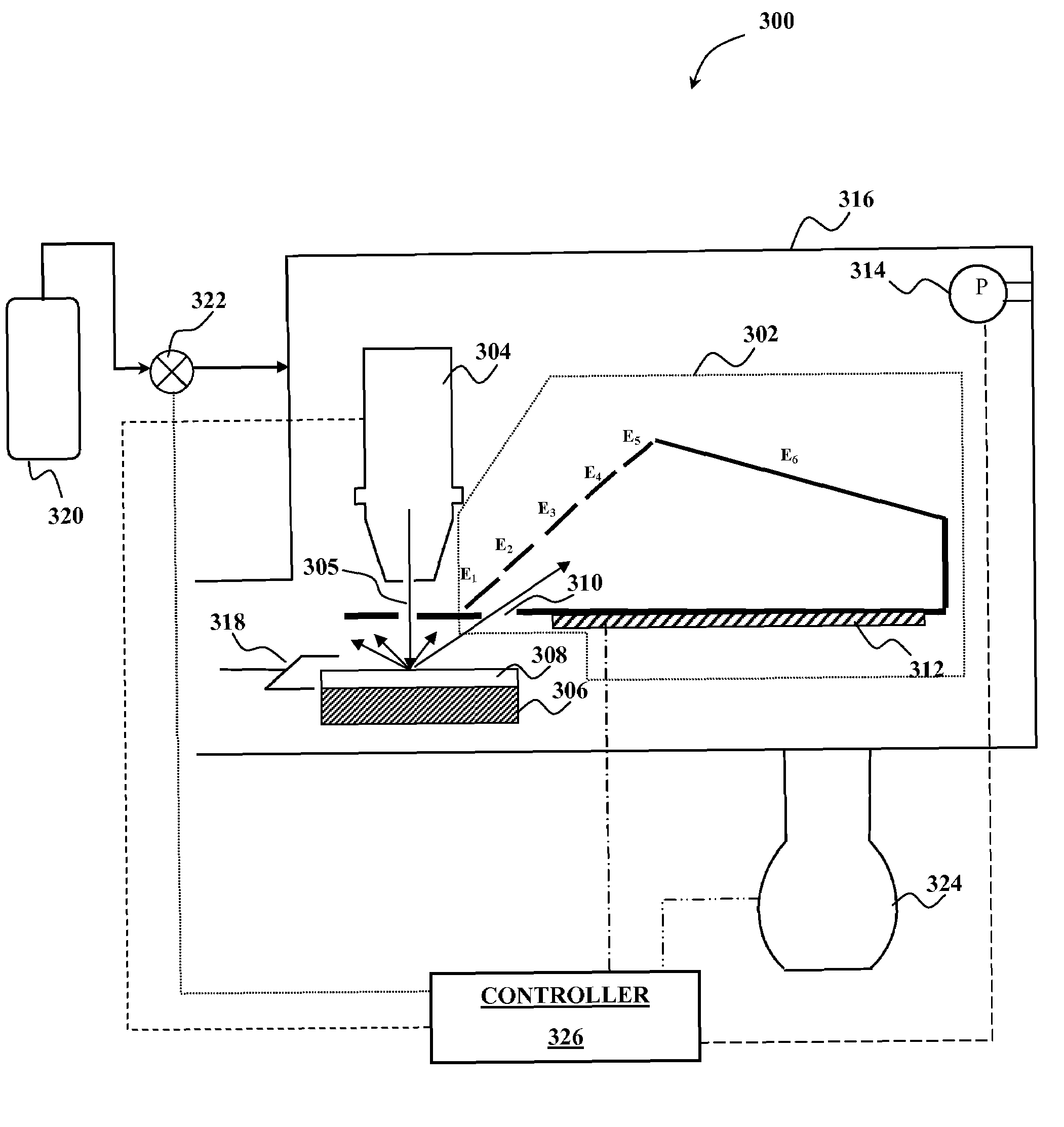
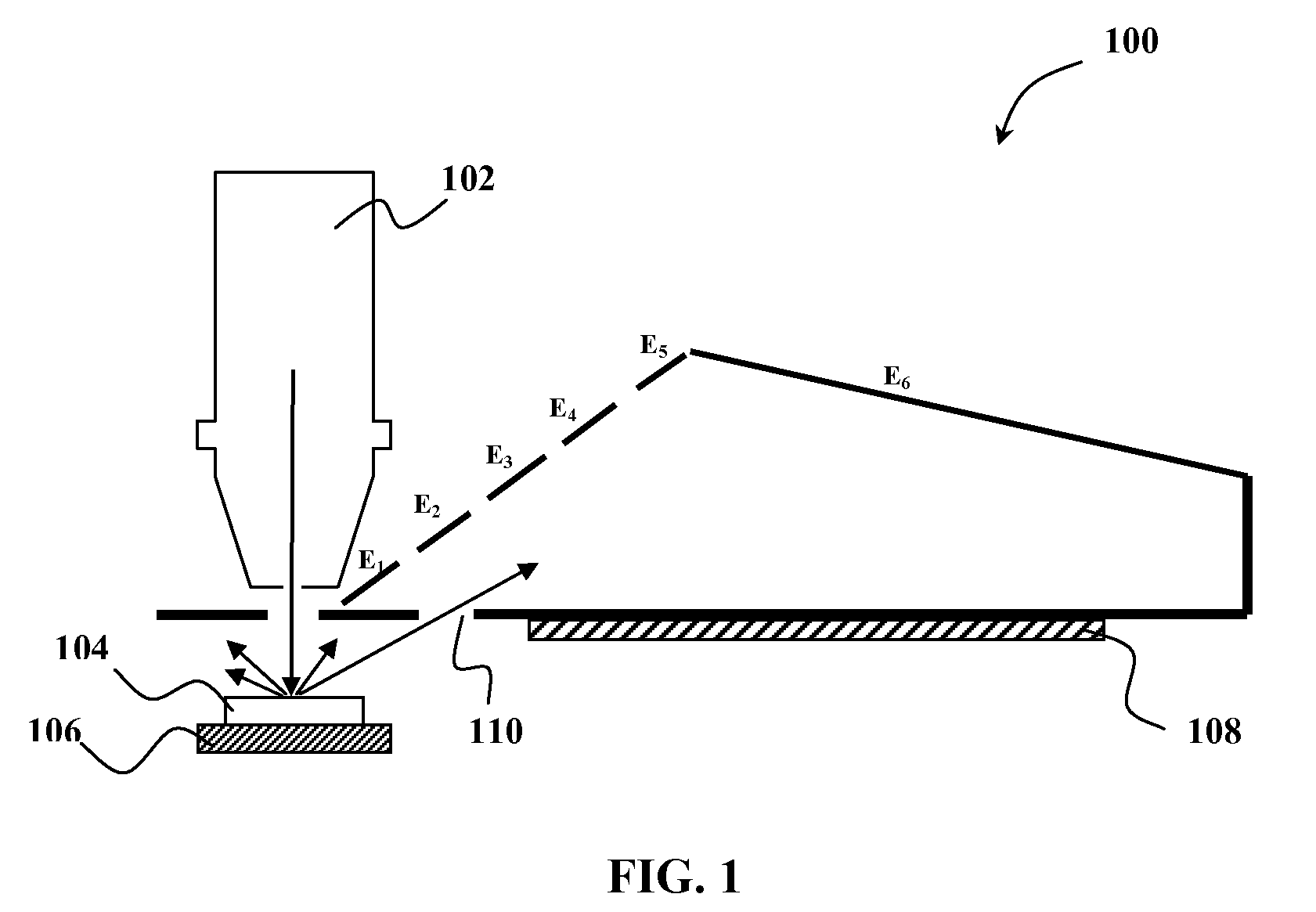
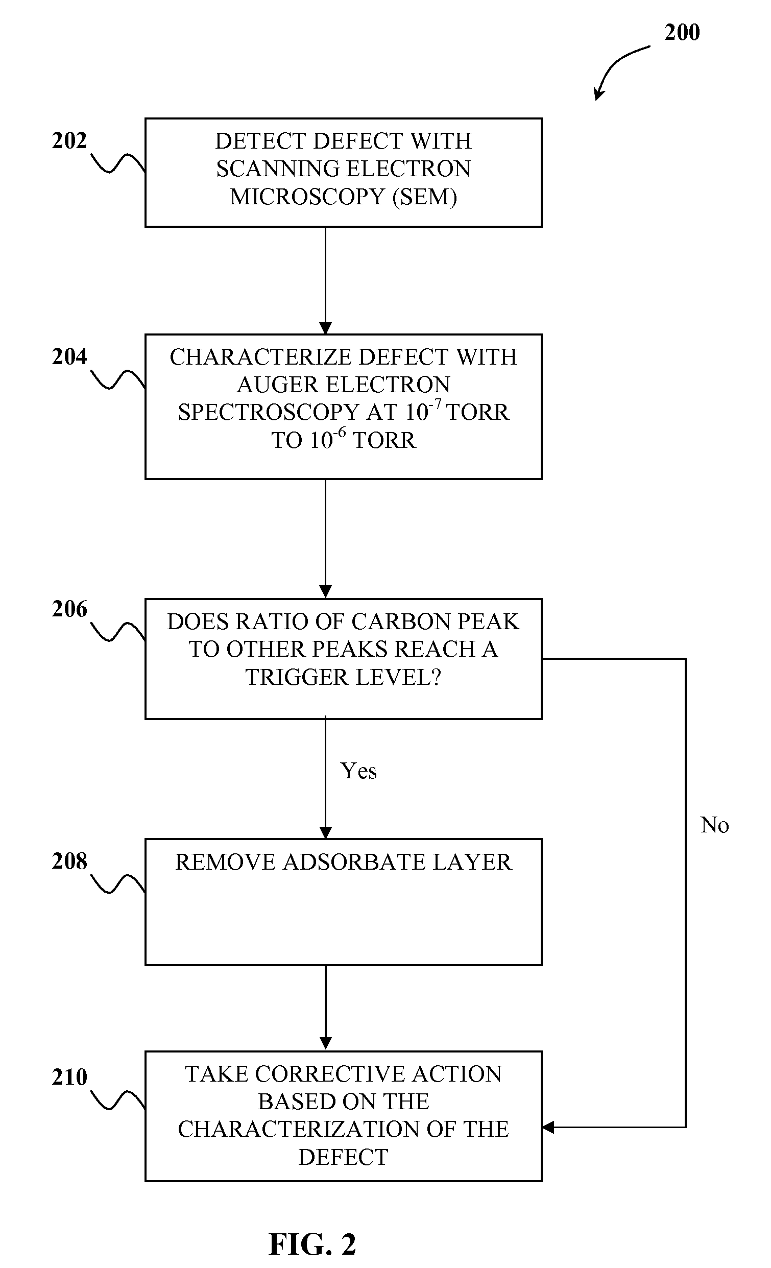
[0015]Defects in a substrate that can be detected by scanning electron microscope (SEM) but are too small to be imaged with the SEM may be chemically characterized using a charged particle spectroscopy technique such as Auger electron spectroscopy. In the art of Auger electron spectroscopy, the electron energy analyzers operate by injecting the diverging electrons into an electric field using a few simply shaped electrodes. Auger electrons of a particular energy injected from the sample into the electric field are deflected by th...


PUM

PropertyMeasurementUnit
sizeaaaaaaaaaa
diameteraaaaaaaaaa
depthaaaaaaaaaa

Abstract

A method and the instrument for characterization of the defects on a surface with Auger electron spectroscopy in a high vacuum environment are disclosed. Defects on the surface of a sample may be characterized with Auger electron spectroscopy in a high vacuum environment.

Description

CLAIM OF PRIORITY[0001]This application claims the benefit of priority of commonly-assigned U.S. Provisional Patent Application No. 60 / 890,512 filed Feb. 19, 2007, the entire contents of which are incorporated herein by reference.FIELD OF THE INVENTION[0002]This invention generally relates to an electron energy analyzing system and more particularly to such a system for Auger electron spectroscopy in high vacuum.BACKGROUND OF THE INVENTION[0003]Over the past few years, the demand for ever cheaper and lighter weight portable electronic devices has led to a growing need to manufacture durable, lightweight, and low cost electronic circuits including high density memory chips. The increasing complexity of electronic devices, and integrated circuits, coupled with the decreasing size of individual circuit elements, places ever more stringent demands on fabrication processes, particularly with respect to the resolution and accuracy of the fabrication patterns. The ability to fabricate on a...

Claims


Application Information

Patent Timeline
Patent Type & Authority Patents(United States)
IPC IPC(8): H01J49/08G01N23/22G01N23/227
CPCG01N23/2276
Inventor NASSER-GHODSI, MEHRANYU, MING LUNFRIEDMAN, STUARTTOTH, GABOR
Owner KLA CORP
Why Eureka
Try Eureka