Switching power supply circuit

a power supply circuit and high frequency technology, applied in the direction of power conversion systems, dc-dc conversion, instruments, etc., can solve the problems of poor response, low processing speed, and earlier technology is difficult to apply to high frequency switching power supply circuits, and achieve the effect of ensuring the stability of an action

Active Publication Date: 2009-12-29
TOREX SEMICON LTD
View PDF12 Cites 12 Cited by
  • Summary
  • Abstract
  • Description
  • Claims
  • Application Information

AI Technical Summary

Benefits of technology

[0013]The present invention has been accomplished in the light of the above-mentioned earlier technologies. It is an object of the present invention to provide a switching power supply circuit capable of ensuring a prompt response to a circuit current, and also ensuring the stability of an action.
[0017]A second aspect of the present invention is the switching power supply circuit according to the first aspect, characterized in that the current mode signal generation means adds the current mode signal to an output of, or an interior of, an error amplifier of the feedback control system, which outputs an error signal representing a differential voltage between a preset reference voltage and a voltage based on the direct current output voltage, such that a duty ratio of the output of the error amplifier is decreased.
[0042]According to the present invention having the above-described features, the current feedback system is constructed by supplying the first current information signal, which is the output signal of the current detection means, to the gate of the first MOS transistor, and utilizing the current mode signal formed by the drain current of the first MOS transistor. That is, the desired current mode signal is formed by the single MOS transistor. Thus, a very quick response can be achieved.

Problems solved by technology

This poses the problem that a processing speed is low and a response is poor.
As a result, this earlier technology has been difficult to apply to a high frequency switching power supply circuit, in particular.
As a result, the influence of the offset voltage of the differential amplifier 6 increases, presenting the problem of rendering the action of the switching power supply circuit unstable.
However, these technologies pose problems similar to those of the earlier technology shown in FIG. 17 that has been described above.
That is, they have the problem of a low processing speed and a poor response.
They encounter the problem, in particular, that their application to a high frequency switching power supply circuit is difficult, and they essentially render the action of the switching power supply circuit unstable.

Method used


Image

  • Switching power supply circuit
  • Switching power supply circuit
  • Switching power supply circuit

Examples


first embodiment

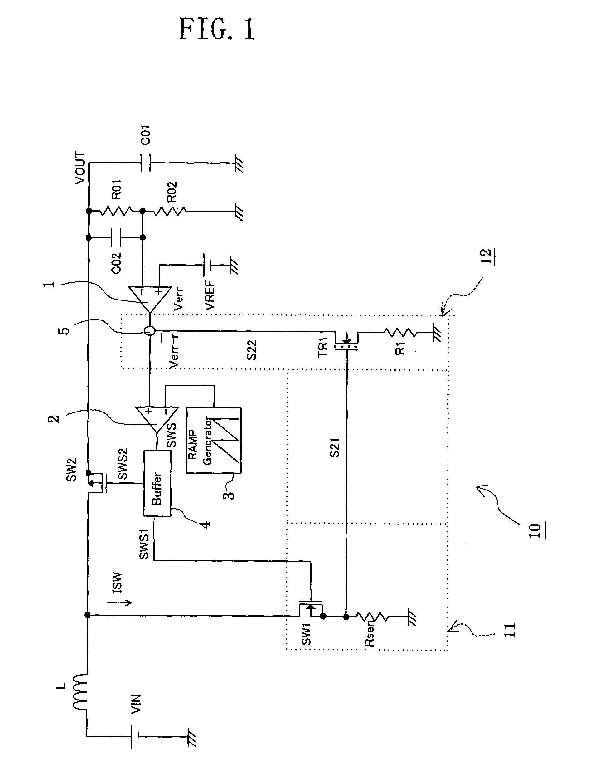
[0062]FIG. 1 is a circuit diagram showing a switching power supply circuit according to a first embodiment of the present invention. As shown in this drawing, the switching power supply circuit according to the present embodiment has a current mode control circuit 10 comprising a current detection means 11 and a current mode signal generation means 12, and the current mode control circuit 10 constitutes a current feedback system.

[0063]In further detail, the current detection means 11 comprises a switching means SW1 and a current detection resistance Rsen connected in series with the switching means SW1, and obtains a first current information signal S21 from the point of connection between the switching means SW1 and the current detection resistance Rsen.

[0064]The current mode signal generation means 12 generates a current mode signal S22 which is the drain current of a first MOS transistor TR1 obtained by supplying the first current information signal S21, as the output signal of t...

second embodiment

[0066]FIG. 2 is a circuit diagram showing a switching power supply circuit according to a second embodiment of the present invention. As shown in this drawing, the present embodiment is a variation of the configuration of the current mode control circuit 10 according to the first embodiment. The other features in the present embodiment are exactly the same as those in the first embodiment. Thus, the same portions as those in FIG. 1 are assigned the same numerals and symbols, and duplicate explanations are omitted.

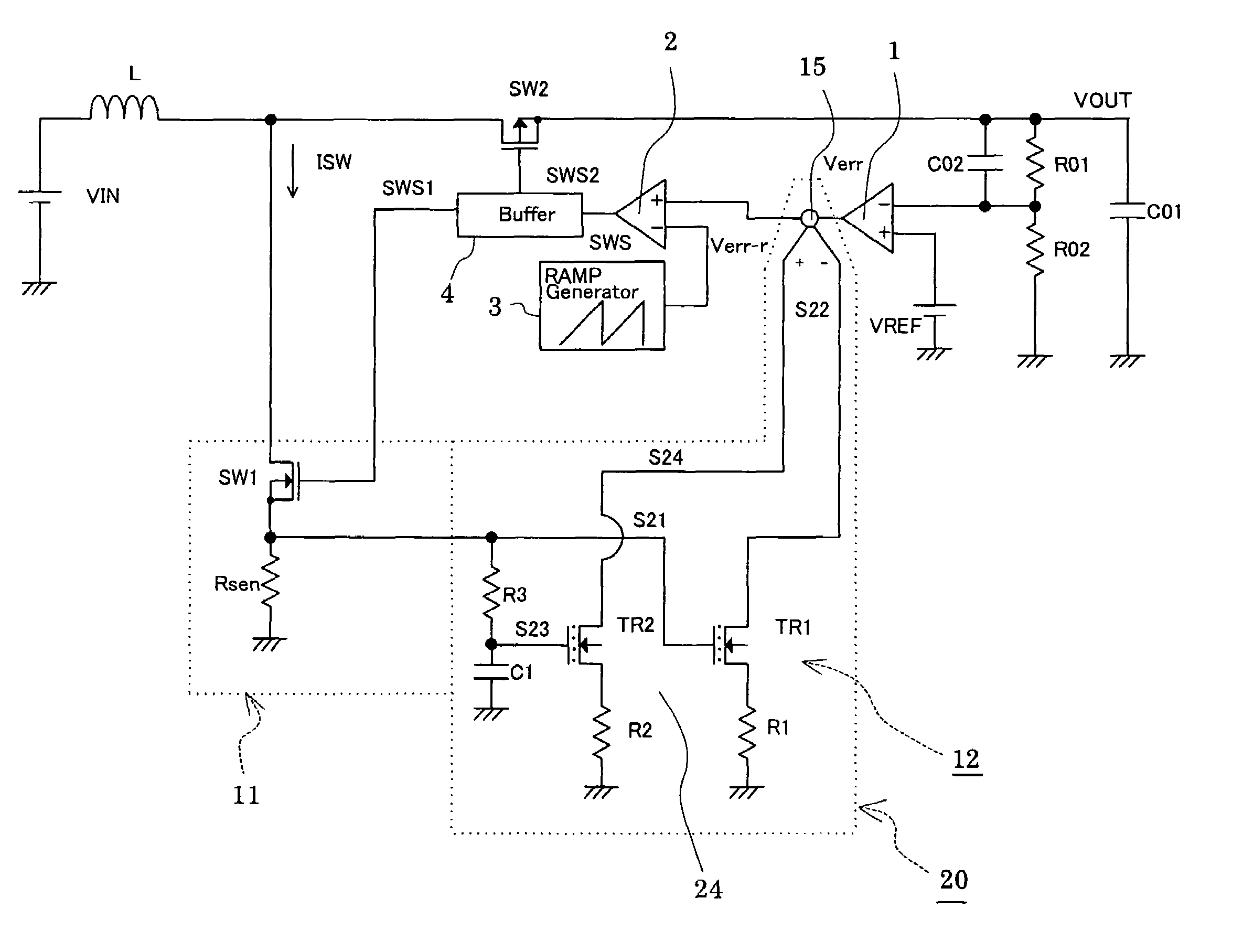
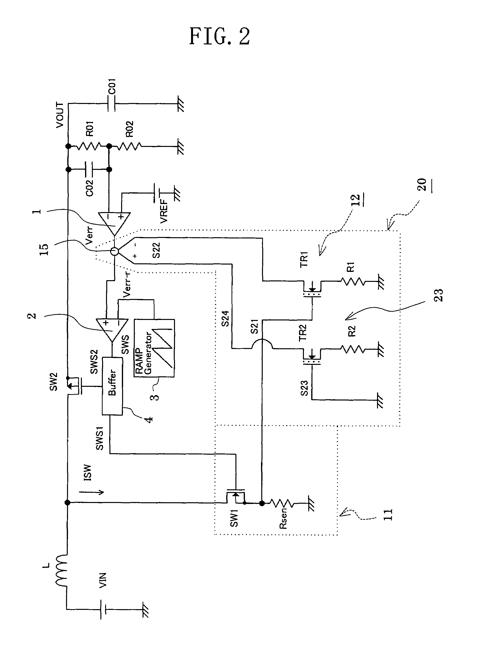
[0067]A current mode control circuit 20 according to the present embodiment has a current correction signal generation means 23 as well as a current mode signal generation means 12. The current correction signal generation means 23 generates a current correction signal S24 for correcting a current mode signal S22 with the drain current of a second MOS transistor TR2 which is obtained by supplying a second current correction signal S23 for a first current information signal ...

third embodiment

[0076]FIG. 4 is a circuit diagram showing a switching power supply circuit according to a third embodiment of the present invention. As shown in this drawing, the present embodiment is a variation of the configuration of the current mode control circuit 20 according to the second embodiment. The other features in the present embodiment are exactly the same as those in the second embodiment. Thus, the same portions as those in FIG. 2 are assigned the same numerals and symbols, and duplicate explanations are omitted.

[0077]A current mode control circuit 30 according to the present embodiment comprises a current mode signal generation means 12 and a current correction signal generation means 23 constituting a current mirror circuit which serves as a current superposition means. That is, the current superposition means is constructed such that a current correction signal S24 is supplied to the gate and drain of a fourth MOS transistor TR4 and the gate of a third MOS transistor TR3, and a...


PUM


Abstract

A switching power supply circuit has a current mode control circuit including current detection means, and current mode signal generation means for generating a current mode signal being a drain current of a first MOS transistor obtained by supplying a first current information signal, which is an output signal of the current detection means, to the gate of the first MOS transistor, and by connecting a first resistance to the source of the first MOS transistor, and supplies the current mode signal to a feedback control system of the switching power supply circuit.

Description

[0001]The entire disclosure of Japanese Patent Application No. 2006-156667 filed Jun. 5, 2006 is expressly incorporated by reference herein.BACKGROUND OF THE INVENTION[0002]1. Field of the Invention[0003]This invention relates to a switching power supply circuit and, more specifically, to a switching power supply circuit useful when detecting a current flowing in the circuit, and providing feedback on current information to obtain a predetermined output voltage.[0004]2. Description of the Related Art[0005]In a switching power supply circuit, a current feedback mode is in wide use for maintaining the stability of the switching power supply circuit.[0006]This type of switching power supply circuit concerned with an earlier technology is shown in FIG. 17. As shown in this drawing, the illustrated switching power supply circuit is a step-up switching power supply circuit, which comprises a switching means SW1 formed from an N-channel MOS transistor, a switching means SW2 formed from a P...

Claims


Application Information

Patent Timeline
Patent Type & Authority Patents(United States)
IPC IPC(8): G05F1/56
CPCH02M3/156H02M2001/0025H02M1/0025
Inventor HANE, NORIMASANAKA, TAKESHI
Owner TOREX SEMICON LTD
Why Eureka
Try Eureka