RF step attenuator

a technology of attenuator and step, which is applied in the direction of diodes, electronic switching, pulse techniques, etc., can solve the problems of high insertion loss and non-linearity, wear and tear of mechanical parts of mechanical attenuators, and high insertion loss of fet devices, etc., to achieve low insertion loss, high attenuation, and low insertion loss

Inactive Publication Date: 2009-12-29
GIGA TRONICS
View PDF2 Cites 8 Cited by
  • Summary
  • Abstract
  • Description
  • Claims
  • Application Information

AI Technical Summary

Benefits of technology

[0001]The present invention relates generally to radio-frequency (RF) attenuators, and more particularly to a high-speed RF step attenuator implemented using long-lifetime PIN diode switches which provides step attenuation across the entire RF frequency spectrum while maintaining minimal insertion loss, return loss, and harmonics.
[0004]Electromechanical relays afford the advantages of high power handling capability, DC coupling, low insertion loss, and isolation of the control signal from the signal being switched. However, mechanical attenuators comprise mechanical parts which wear out over time, and are often unreliable due to environmental noise, such as vibration.
[0007]PIN diodes offer low cost, fast switching speed, and high reliability. The disadvantage to utilizing PIN diodes is their characteristically high insertion loss. Furthermore, when used as switches in attenuators, they are bandwidth limited and generate undesired harmonics.
[0009]It would therefore be desirable to have available a broadband, high-attenuation, high-frequency-switching-speed RF step attenuator that is characterized by low insertion loss, low return loss, and minimal harmonics.SUMMARY OF THE INVENTION
[0010]Embodiments of the invention include fully electronic high-speed switches characterized by low insertion loss and minimal harmonics, and a broadband, high attenuation step attenuator characterized by low insertion loss, low return loss, and minimal harmonics.

Problems solved by technology

However, mechanical attenuators comprise mechanical parts which wear out over time, and are often unreliable due to environmental noise, such as vibration.
FET devices have the potential drawbacks of characteristically high insertion loss and non-linearity, particularly at the lower end of the RF frequency spectrum.
The disadvantage to utilizing PIN diodes is their characteristically high insertion loss.
Furthermore, when used as switches in attenuators, they are bandwidth limited and generate undesired harmonics.
Because of the aforementioned limitations of the available switching devices, and because the RF spectrum is so broadband, there are many challenges in building a step attenuator that provides sufficient attenuation across the entire RF spectrum.

Method used


Image

  • RF step attenuator
  • RF step attenuator
  • RF step attenuator

Examples


Embodiment Construction

[0022]Embodiments of the invention include fully electronic high-speed switches characterized by low insertion loss and minimal harmonics, and a broadband, high attenuation step attenuator characterized by low insertion loss, low return loss, and minimal harmonics.

[0023]In an embodiment, the step attenuator meets the RF specifications listed in Table 1.

[0024]

TABLE 1ParameterUnitSpecification LimitFrequency RangeFminMHz4.0FmaxGHz8.0Attenuation Range (in 10dB110dB steps)Attenuation FlatnessdB±0.25(over any 100 MHzBandwidth)Maximum Input PowerdBm27Insertion Loss4 MHzdB10.01 GHzdB2.53 GHzdB7.08 GHzdB10.0Harmonics (10 dBmdBc−57input)Return LossdB20Switching Speed□sec100

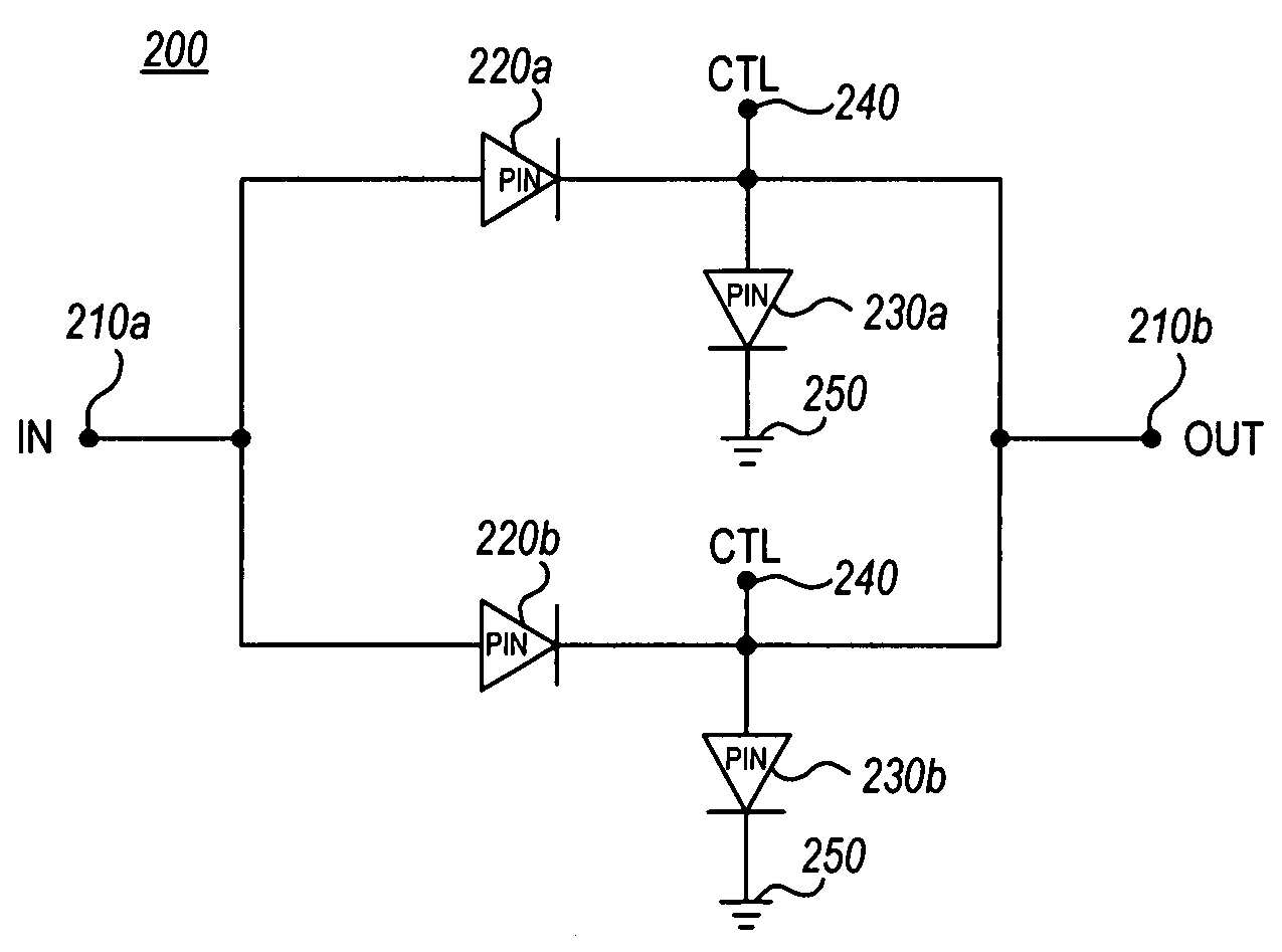
[0025]FIG. 1 illustrates a “series” attenuator configuration which may be utilized in a step attenuator 100 along a transmission line 110. As illustrated, the series attenuator configuration is characterized by a plurality of attenuator pads 101, 102, 103, 104, each of which can be serially interconnected in the circuit, o...


PUM


Abstract

A broadband, high-speed RF step attenuator implemented using long-lifetime PIN diode switches is presented which provides step attenuation across a significant portion of the entire RF frequency spectrum while maintaining minimal insertion loss, return loss, and harmonics.

Description

[0001]The present invention relates generally to radio-frequency (RF) attenuators, and more particularly to a high-speed RF step attenuator implemented using long-lifetime PIN diode switches which provides step attenuation across the entire RF frequency spectrum while maintaining minimal insertion loss, return loss, and harmonics.[0002]Electronic signal step attenuators are used in a variety of electronic applications to reduce the power level of an electronic signal for use by other electronic components or instruments requiring lower power signals. Step attenuators rely on switches to selectably couple one or more attenuator pads (also known as “sections”) into the circuit.[0003]In RF attenuators, the switches are generally activated by control signals which may be toggled by a computer or other control device. Among the switches commonly used in step attenuators are electromechanical RF relays, FET switches, and PIN diode switches.[0004]Electromechanical relays afford the advanta...

Claims


Application Information

Patent Timeline
Patent Type & Authority Patents(United States)
IPC IPC(8): H01P1/22H01P1/10H03H7/24
CPCH01P1/227
Inventor FUENTES, CARLOS
Owner GIGA TRONICS
Why Eureka
Try Eureka