An optoelectronic semiconductor device

a technology of optoelectronic and semiconductor devices, applied in the field of optoelectronic semiconductor devices, can solve the problems of lack of integrated laser sources, further costly and waste, and the field of optoelectronics has also faced a big stumbling block

Pending Publication Date: 2022-08-11
UNIV COLLEGE OF LONDON +1
View PDF0 Cites 0 Cited by
  • Summary
  • Abstract
  • Description
  • Claims
  • Application Information

AI Technical Summary

Problems solved by technology

Problems associated with the known fabrication techniques are that they are costly due to the manipulation required to integrate group III/V dies onto the silicon chip, and also because most of the group III/V compound semiconductor material is removed in the integration process, which is further costly and wasteful.
Furthermore, amid all of the complex circuitry implemented on known silicon-based photonics and the possibilities offered by known silicon proces

Method used


Image

  • An optoelectronic semiconductor device
  • An optoelectronic semiconductor device
  • An optoelectronic semiconductor device

Examples


Embodiment Construction

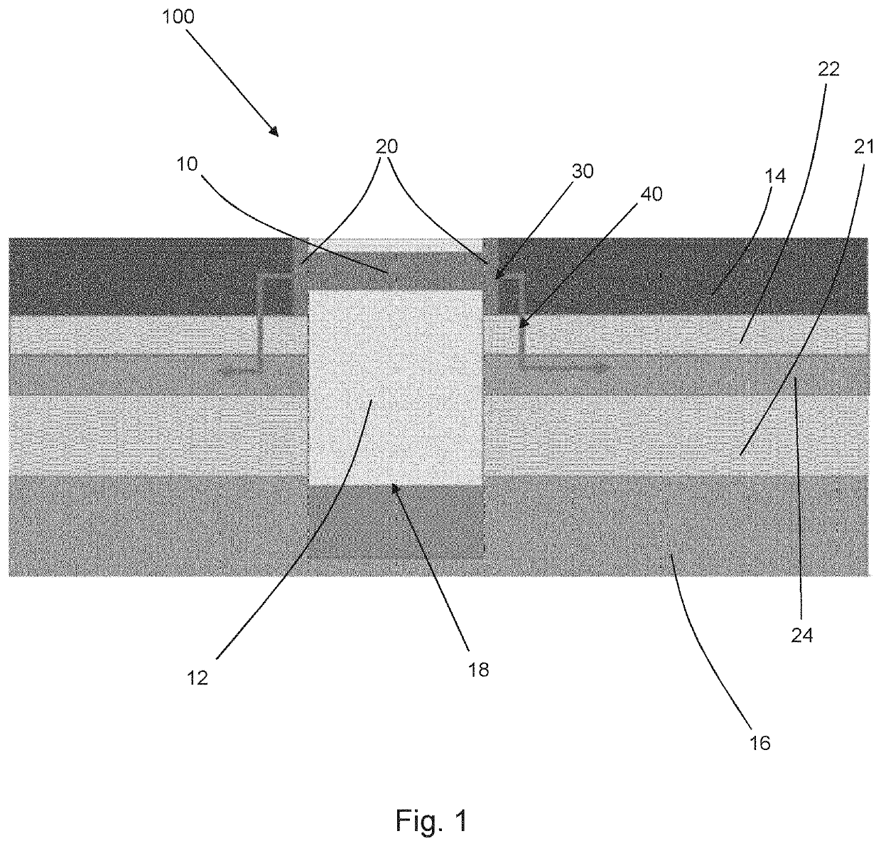
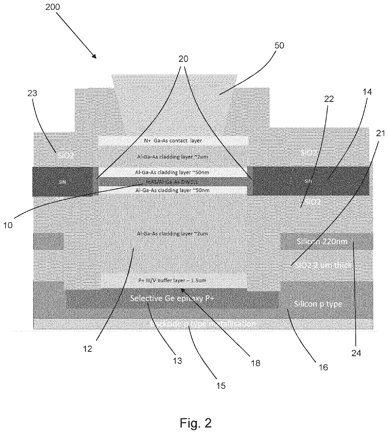
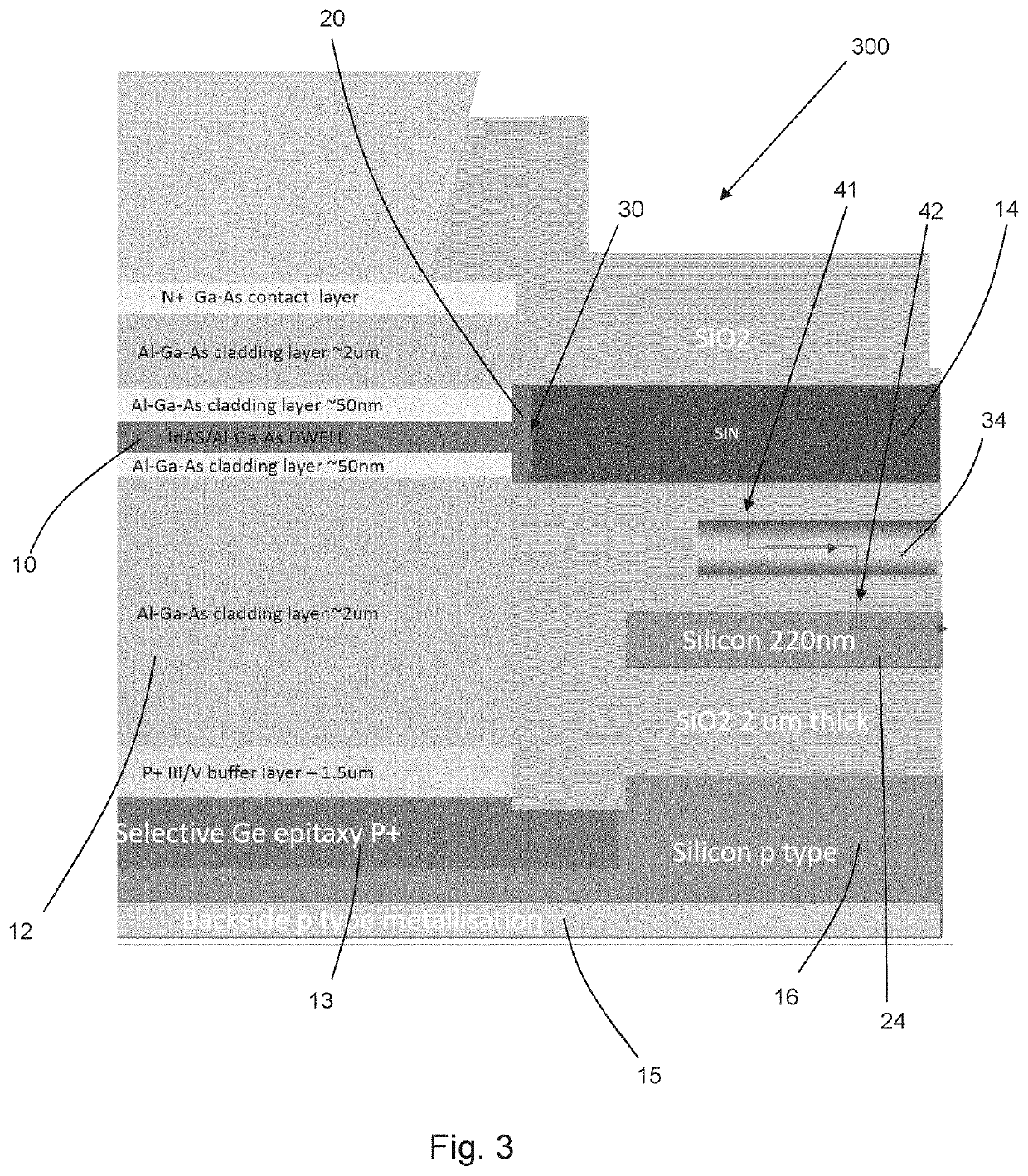
[0046]FIG. 1 is a cross-sectional view showing a semiconductor device 100 for use in an optoelectronic integrated circuit, according to an embodiment of the present invention. The semiconductor device 100 is made from multiple internal layers that include at least a group IV substrate (or substrate layer) 16, a waveguide 14, and a group III / V multilayer stack 12.

[0047]The height of a device is measured in a direction away from the substrate 16. A top surface of a device is the surface that is farthest from the substrate 16 and a bottom surface of a device is the surface that is closest to the substrate 16. A width of a device is measured in a direction perpendicular to the height and perpendicular to the direction of propagation of light along the waveguide 14. A length of a device is measured in a direction perpendicular to the height and parallel to the direction of the propagation of light along the waveguide 14.

[0048]Referring to FIG. 1, the substrate 16 is located at the bottom...


PUM


Abstract

A semiconductor device for use in an optoelectronic integrated circuit; the device comprising: a group four substrate, a waveguide, and a group III/V multilayer stack; wherein the group III/V multilayer stack comprises a quantum component for producing light for the waveguide; wherein the waveguide comprises a material with a deposition temperature below 550 degrees Celsius and a refractive index of any value between 1.3 and 3.8.

Description

FIELD OF THE INVENTION[0001]One or more aspects of embodiments according to the present invention relate to semiconductor devices and their integration with waveguides and other devices to form optoelectronic integrated circuits, and a method of fabrication of the same.BACKGROUND OF THE INVENTION[0002]Lasers, particularly quantum lasers, have many well-documented uses in optoelectronic integrated circuit applications, such as being a crucial component of an optical interconnect, for example. As such, a laser's output power, reliability, linewidth and power efficiency are key performance metrics. For these reasons at least, quantum lasers are used as they exploit the benefits associated with quantum confinement of charge carriers (i.e. electrons and / or electron holes), such as yielding a desired gain spectrum or requiring a lower threshold current.[0003]It is known in the field that group III / V compound semiconductor material lasers (hereafter referred to as group III / V lasers) are i...

Claims


Application Information

Patent Timeline
IPC IPC(8): H01S5/343G02B6/12G02B6/13H01S5/02H01S5/026H01S5/34
CPCH01S5/343G02B6/12004G02B6/131G02B2006/12061H01S5/026H01S5/341H01S5/021H01L33/06
Inventor GARDES, FREDERICSEEDS, ALWYN JOHNLIU, HUIYUNCHEN, SIMING
Owner UNIV COLLEGE OF LONDON
Why Eureka
Try Eureka