Low-loss mm-wave CMOS resonant switch

a resonant switch, low-loss technology, applied in electronic switching, pulse technique, electrical equipment, etc., can solve the problems of inability to penetrate solid obstacles, limited transmission distance of such signals, and inability to integrate on-die components

Active Publication Date: 2022-09-06
MOBIX LABS INC
View PDF83 Cites 0 Cited by
  • Summary
  • Abstract
  • Description
  • Claims
  • Application Information

AI Technical Summary

Benefits of technology

[0009]The present disclosure is directed to RF (radio frequency) switches exhibiting minimal insertion losses at mmWave operating frequencies. The switch may be configured such that the metallic trace losses contribute primarily to the insertion loss while activated, and a parallel resonant circuit being present while deactivated. Furthermore, magnetic flux cancellation and consecutive self-inductance minimization is contemplated.

Problems solved by technology

Although the higher operating frequency bands, and mmWave / FR2 in particular, offer the highest data transfer speeds, the transmission distance of such signals may be limited.
Furthermore, signals at this frequency range may be unable to penetrate solid obstacles.
This is particularly problematic with integrated on-die components.
There are several known deficiencies with this configuration, however.
A large value inductor, in turn, results in significant series losses and losses associated with shunting to ground.
A smaller transistor size results in higher series losses but lower losses associated with shunting to ground via lossy substrate.

Method used


Image

  • Low-loss mm-wave CMOS resonant switch
  • Low-loss mm-wave CMOS resonant switch
  • Low-loss mm-wave CMOS resonant switch

Examples


first embodiment

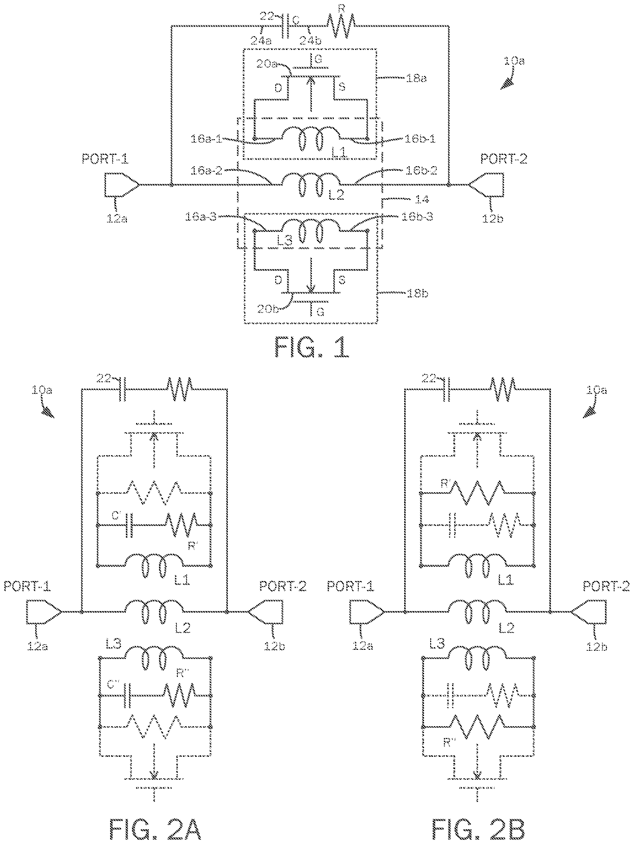
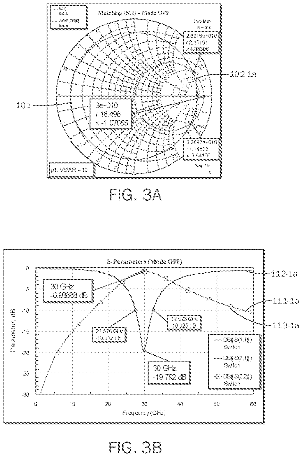
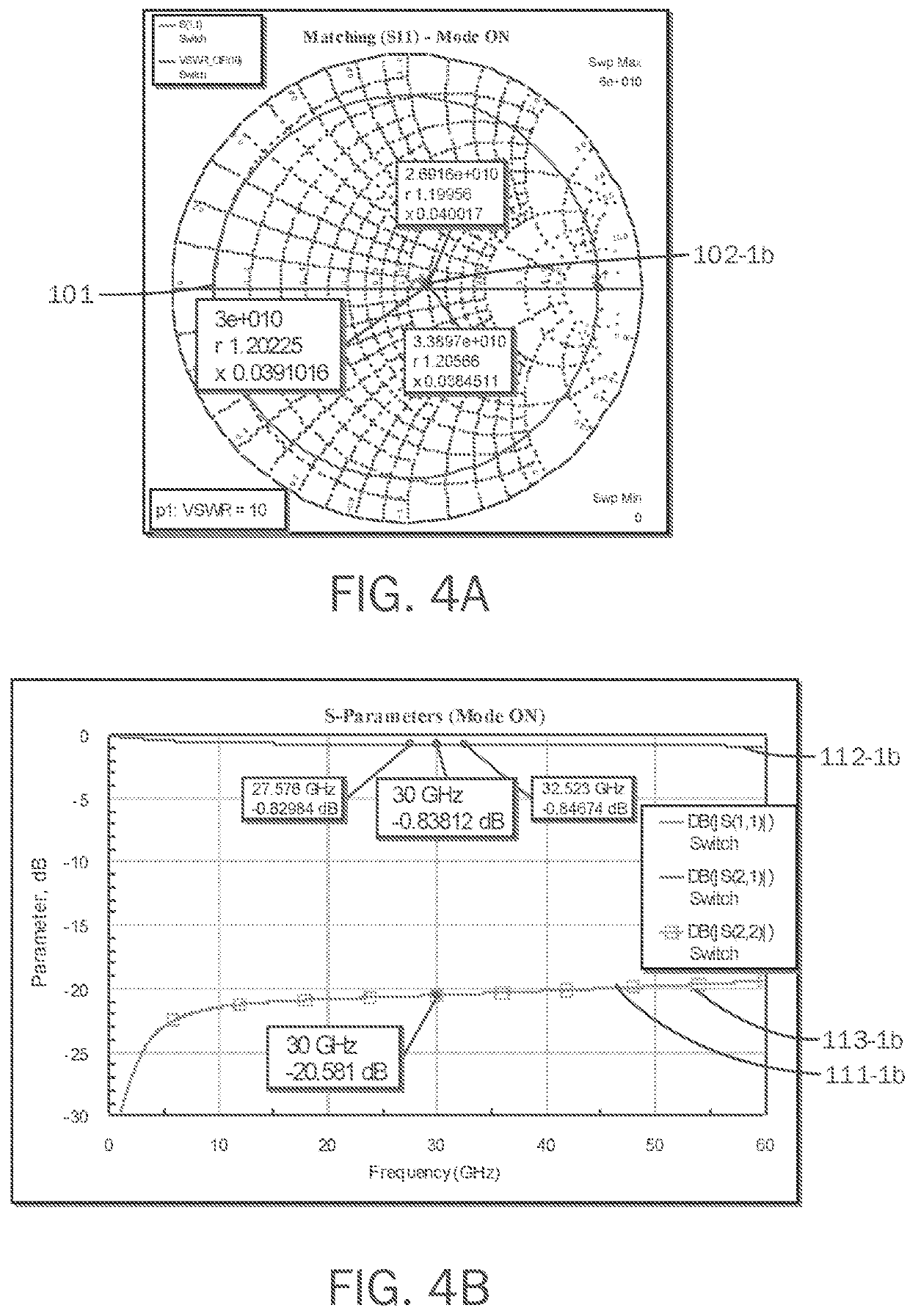
[0063]Referring now to the schematic diagram of FIG. 1, a resonant switch 10a is generally defined by a first port 12a and a second port 12b, to which various other circuit components may be connected. In general, the resonant switch 10 selectively connects those components that are directly connected to the first port 12a, to those components that are directly connected to the second port 12b.

[0064]Various embodiments of the resonant switch 10 incorporate a triple inductor network 14, which may be comprised of a center inductor L2, a first peripheral inductor L1, and a second peripheral inductor L3. The center inductor L2 is defined by a first terminal 16a-2 that is electrically connected to the first port 12a, and a second terminal 16b-2 that is electrically connected to the second port 12b. The first peripheral inductor L1 likewise has a first terminal 16a-1 and a second terminal 16b-1, while the second peripheral inductor L2 has a first terminal 16a-3 and a second terminal 16b-...

second embodiment

[0090]The peripheral inductors L1, L3 are a part of the one transistor switch 18 that is a constituent element of the resonant switch 10. In the illustrated embodiment, the transistor switch 18 has a single transistor 20. In the illustrated second embodiment of the resonant switch 10b, the transistor 20 is contemplated to be a field effect transistor that has a gate terminal, a drain terminal, and a source terminal. More specifically, such a field effect transistor is understood to be a MOSFET transistor. In the illustrated example, the transistor 20 is of the N-type, that is, having an n-type drain and source, and a p-type substrate. This is by way of example only and not of limitation, and P-type transistors may be substituted if desired. Moreover, the specific fabrication technology need not be limited to metal oxide semiconductor, and any other suitable transistor type may be substituted in the transistor switch 18.

[0091]In the transistor switch 18, the drain terminal of the tra...

third embodiment

[0115]The peripheral inductors a part of transistor switches 18 that are a constituent element of the resonant switch 10. There is a first transistor switch 18a that incorporates the first peripheral inductor L1, and a second transistor switch 18b that incorporates the second peripheral inductor L3. In one embodiment, the first transistor switch 18a has first transistor 20a-1 and a second transistor 20a-2 that are connected in series, and the second transistor switch 18b has a first transistor 20b-1 and a second transistor 20b-2 that are similarly connected in series. In the illustrated third embodiment of the resonant switch 10c, the transistors 20 are contemplated to be field effect transistors that have a gate terminal, a drain terminal, and a source terminal. The specific fabrication technology need not be limited to metal oxide semiconductor as shown, and any other suitable transistor type may be substituted in the transistor switches 18.

[0116]In the first transistor switch 18a...


PUM


Abstract

A resonant switch with a first port and a second port has a capacitor connected thereto. A triple inductor network has a center inductor connected to the first port and the second port, and first and second peripheral inductors each electromagnetically coupled thereto. In a deactivated state, the center inductor and the capacitor define a parallel resonance at a predefined operating frequency range, and in an activated state, insertion loss associated with the center inductor is substantially minimized to metallic trace loss attributable thereto.

Description

CROSS-REFERENCE TO RELATED APPLICATIONS[0001]This application relates to and claims the benefit of U.S. Provisional Application No. 63 / 059,042, filed Jul. 30, 2020 and entitled “LOW-LOSS MM-WAVE CMOS RESONANT SWITCH”, the disclosure of which is wholly incorporated by reference in its entirety herein.STATEMENT RE: FEDERALLY SPONSORED RESEARCH / DEVELOPMENT[0002]Not ApplicableBACKGROUND1. Technical Field[0003]The present disclosure relates generally to radio frequency (RF) integrated circuits, and more particularly, to low-loss millimeter wave complementary metal oxide semiconductor resonant switches.2. Related Art[0004]Wireless communications systems find applications in numerous contexts involving information transfer over long and short distances alike, and a wide range of modalities tailored for each need have been developed. Chief among these systems with respect to popularity and deployment is the mobile or cellular phone. Generally, wireless communications utilize a radio frequen...

Claims


Application Information

Patent Timeline
Patent Type & Authority Patents(United States)
IPC IPC(8): H04B1/00H04B1/44H04B1/46H04B1/48H03K17/693H03K17/687
CPCH03K17/693H03K17/6872H03K2217/0054
Inventor GORBACHOV, OLEKSANDRZHANG, LISETTE L.
Owner MOBIX LABS INC
Why Eureka
Try Eureka