Probe and method of manufacturing probe

a manufacturing method and probe technology, applied in the field of probes, can solve the problems of decreasing the stylus pressure, unstable continuity between the probe and the electrode pad, and the risk of damaging the wiring layer and the insulation layer, so as to ensure and stabilize the inspection of an obj

Inactive Publication Date: 2010-01-19
OCTEC INC +1
View PDF24 Cites 7 Cited by
  • Summary
  • Abstract
  • Description
  • Claims
  • Application Information

AI Technical Summary

Benefits of technology

[0016]According to the present invention, it is possible to provide a probe enabling sure and stable inspection of an object to be inspected with a low stylus pressure by breaking an oxide film, and a method of manufacturing the same.

Problems solved by technology

However, in recent years, in accordance with sophistication of functions and speed increase of an integrated circuit, a wiring structure has rapidly become more microscopic and thinner and a wiring layer has become extremely thin, and therefore, giving a stylus pressure to the probe for the inspection as described in the conventional patent document 1 involves a risk of damaging a wiring layer and an insulation layer because the probe penetrates not only the oxide film but also the wiring layer or because of a concentration stress from the probe.
On the contrary, decreasing the stylus pressure involves a risk of causing unstable continuity between the probe and the electrode pad.
Further, though the bumps described in the patent documents 2, 3 can surely break the oxide film of an electrode pad by the irregularities, it involves a risk of damaging the wiring layer and the insulation layer depending on the stylus pressure, similarly to the case of the patent document 1.

Method used


Image

  • Probe and method of manufacturing probe
  • Probe and method of manufacturing probe
  • Probe and method of manufacturing probe

Examples


Embodiment Construction

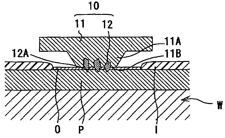
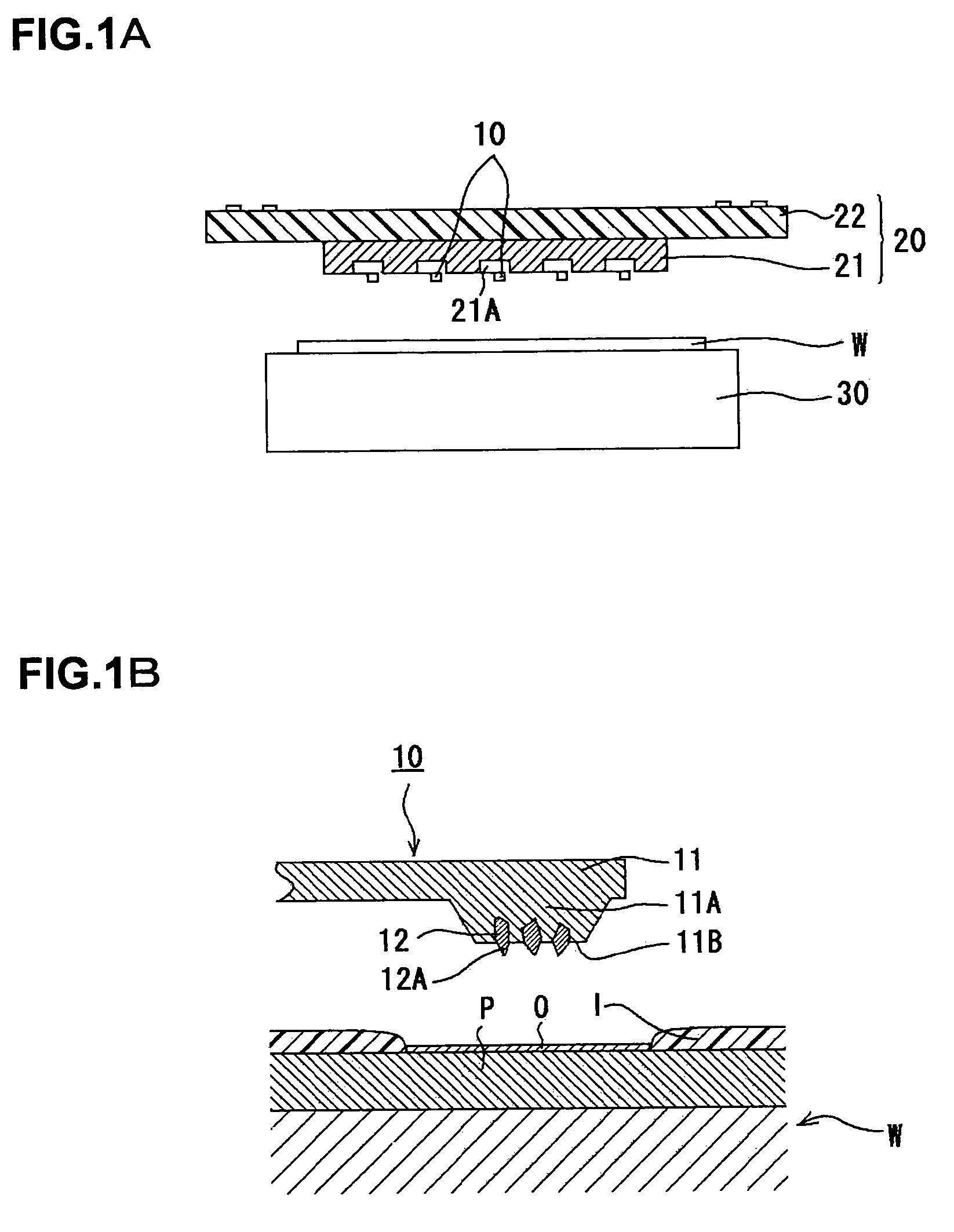
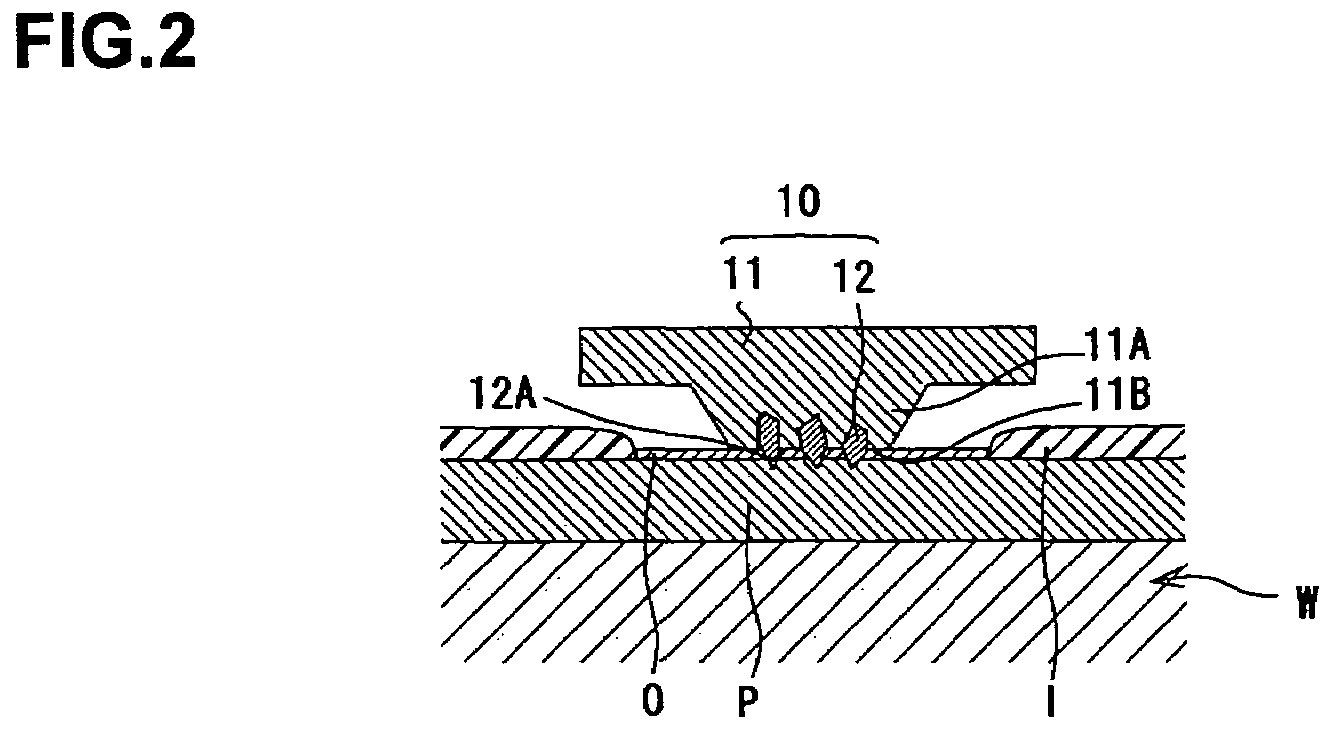
[0029]Hereinafter, the present invention will be described based on embodiments shown in FIG. 1 to FIG. 3. FIGS. 1(a) and (b) are views showing an embodiment of the probe of the present invention, (a) being a cross-sectional view showing a probe card to which the probe is applied and (b) being a cross-sectional view showing an essential part of the probe, FIG. 2 is a cross-sectional view showing a state in which the probe and an electrode pad shown in FIG. 1 are in electrical contact with each other, and FIGS. 3(a) to (e) are cross-sectional views showing essential parts of manufacturing steps of the probe shown in FIG. 1.

[0030]When in use, probes 10 of this embodiment are attached to a probe card 20 as shown in, for example, FIG. 1(a). As shown in the drawing, the probe card 20 includes a contactor 21 formed of, for example, a ceramic substrate, and a printed wiring board 22 electrically connected to the contactor 21, and is structured to inspect electrical characteristics of a plu...


PUM

PropertyMeasurementUnit
diameteraaaaaaaaaa
diameteraaaaaaaaaa
thicknessaaaaaaaaaa

Abstract

In accordance with an increase in speed, a wiring structure has rapidly become more microscopic and thinner and a wiring layer has become extremely thin, and therefore, giving a contact load to a probe for the inspection as has been conventionally done causes damage to a wiring layer and an insulation layer because the probe penetrates not only the oxide film but also the wiring layer or because of a concentration stress from the probe. On the other hand, decreasing the contact load causes unstable continuity between the probe and an electrode pad.It is an object of the present invention to surely and stably inspect an object to be inspected by breaking an oxide film with a low stylus pressure.The present invention is a probe that comes into electrical contact with an object to be inspected when inspecting an electrical characteristic of the object to be inspected, the probe including: a probe main body having a contact portion that comes into contact with the object to be inspected; and a plurality of conductive materials having tip portions projecting from the contact portion of the probe main body.

Description

CROSS REFERENCE TO RELATED APPLICATIONS[0001]This application is a National Phase Application of International Application No. PCT / JP2005 / 003609, filed Mar. 3, 2005, and claims the priority of Japanese Patent Application No. 2004-063228, filed Mar. 5, 2004, the content of both of which is incorporated herein by reference.TECHNICAL FIELD[0002]The present invention relates to a probe used for inspecting an electrical characteristic of an object to be inspected such as a wafer, and more particularly, to a probe enabling inspection with a less stylus pressure.BACKGROUND ART[0003]For inspecting an electrical characteristic of an object to be inspected such as a wafer, an inspection device such as, for example, a probe device is used. The inspection device is provided with a probe card coming into electrical contact with the object to be inspected, and inspects electrical characteristics of IC chips formed on the object to be inspected by bringing a plurality of probes attached to the pro...

Claims


Application Information

Patent Timeline
Patent Type & Authority Patents(United States)
IPC IPC(8): G01R31/02G01R31/28G01R1/067G01R1/073G01R31/26H01L21/66
CPCG01R1/06738Y10T29/5193G01R3/00G01R1/067H01L22/00B82Y30/00
Inventor OKUMURA, KATSUYAYONEZAWA, TOSHIHIRO
Owner OCTEC INC
Why Eureka
Try Eureka