Semiconductor device and method of producing the same

a technology of semiconductor and post electrode, which is applied in the direction of semiconductor devices, semiconductor/solid-state device details, electrical apparatus, etc., can solve the problems of difficult to accurately produce semiconductor, difficult to arrange a large number of wirings between the post electrodes, and the configuration surrounding the post electrode becomes more complicated, etc., to achieve simple shape, small variance in shape due to overlap accuracy relative to the base portion, and large area

Inactive Publication Date: 2010-01-26
LAPIS SEMICON CO LTD
View PDF7 Cites 0 Cited by
  • Summary
  • Abstract
  • Description
  • Claims
  • Application Information

AI Technical Summary

Benefits of technology

[0014]Accordingly, when a plurality of electrodes is arranged in a row, the base portion is not shifted from one of the electrodes toward another of the electrodes next to the one of the electrodes. As a result, it is possible to obtain a large area between the electrodes, and to accommodate a large number of wirings.
[0015]After the electrode is formed, the base portion is completely covered with the electrode. As a result, the electrode including the base portion has a simple shape, and a variance in the shape due to overlapping accuracy relative to the base portion becomes small.

Problems solved by technology

Accordingly, it is difficult to arrange a large number of wirings between the post electrodes.
Further, when the wiring is made smaller to accommodate an increased number of wirings, it is difficult to accurately produce the semiconductor.
Further, a configuration surrounding the post electrode becomes more complicated, and a shape varies to larger extent.

Method used


Image

  • Semiconductor device and method of producing the same
  • Semiconductor device and method of producing the same
  • Semiconductor device and method of producing the same

Examples


first embodiment

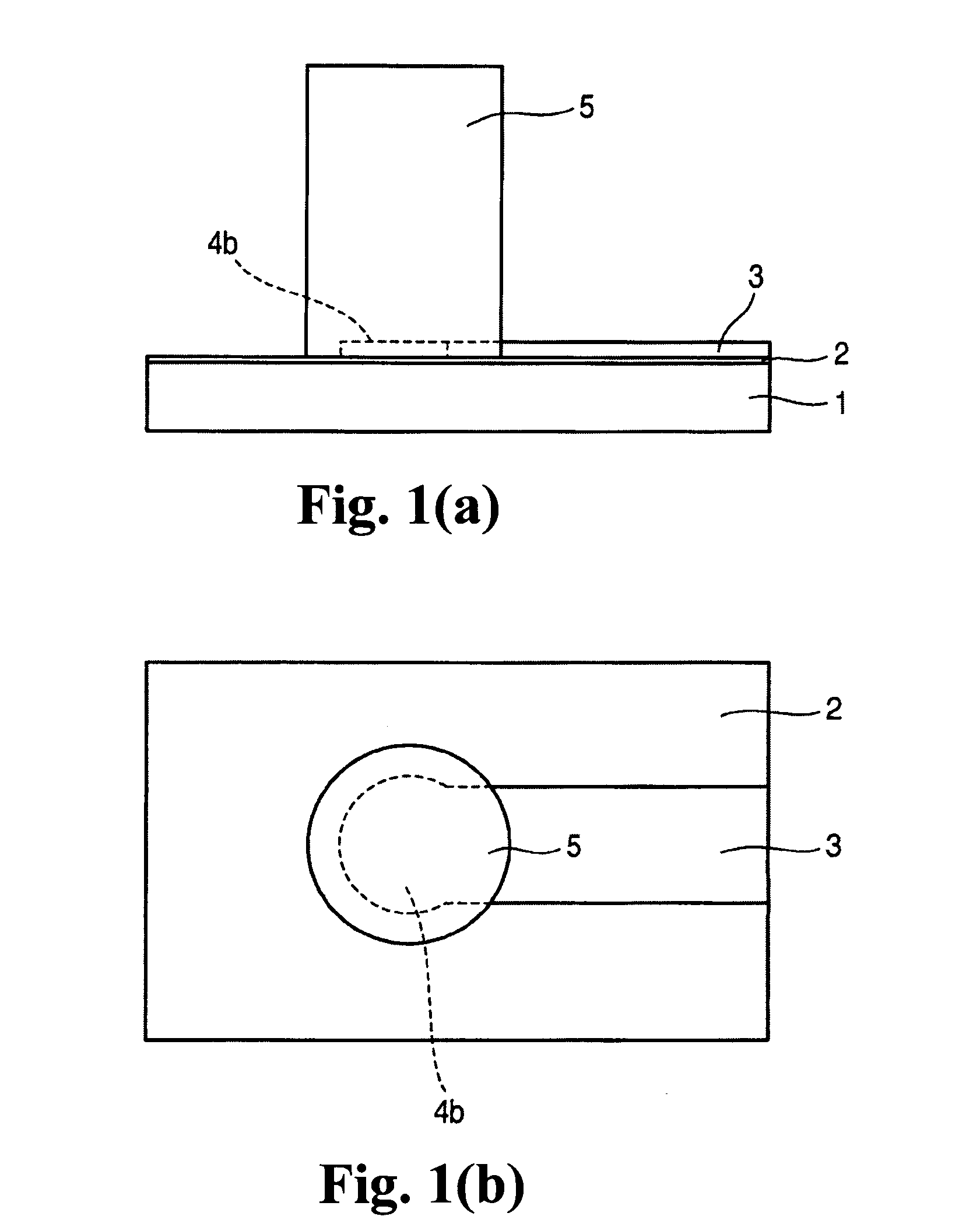
[0021]FIGS. 1(a) and 1(b) are schematic views showing a post electrode according to a first embodiment of the present invention, wherein FIG. 1(a) is a side view thereof, and FIG. 1(b) is a plan view thereof. A semiconductor device after the post electrode is formed and before a seed layer is etched is shown in FIGS. 1(a) and 1(b).

[0022]As shown in FIG. 1(a), an organic insulation layer 1 is formed on a passivasion layer of a wafer (substrate) having an integrated circuit (not shown) formed thereon. The organic insulation layer 1 may be formed of a material such as a polyimide resin, a BCB resin, and a PBO resin. A seed layer 2 is formed of metal such as tungsten, nickel, and chrome, so that plating current flows in a pattern formed with photolithography when a wiring or post electrode is plated.

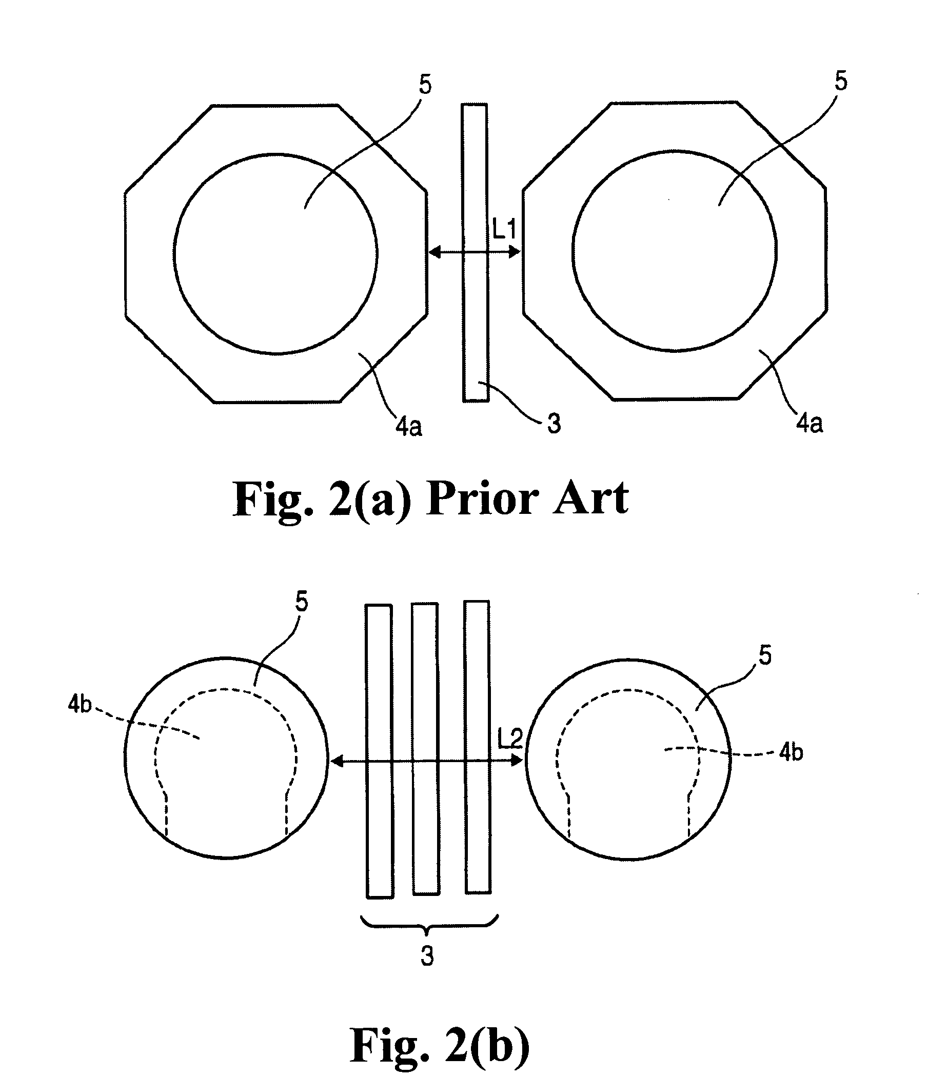
[0023]A wiring 3 is provided for electrically connecting a pad of an integrated circuit (not shown) and a post electrode 5 (described later). The wiring 3 includes a base portion 4b, and is ...

second embodiment

[0039]A second embodiment of the present invention will be explained next. FIGS. 3(a) and 3(b) are schematic views according to a second embodiment of the present invention, wherein FIG. 3(a) is a side view, and FIG. 3(b) is a plan view. Components in the second embodiment same as those in the first embodiment are designated by the same reference numerals.

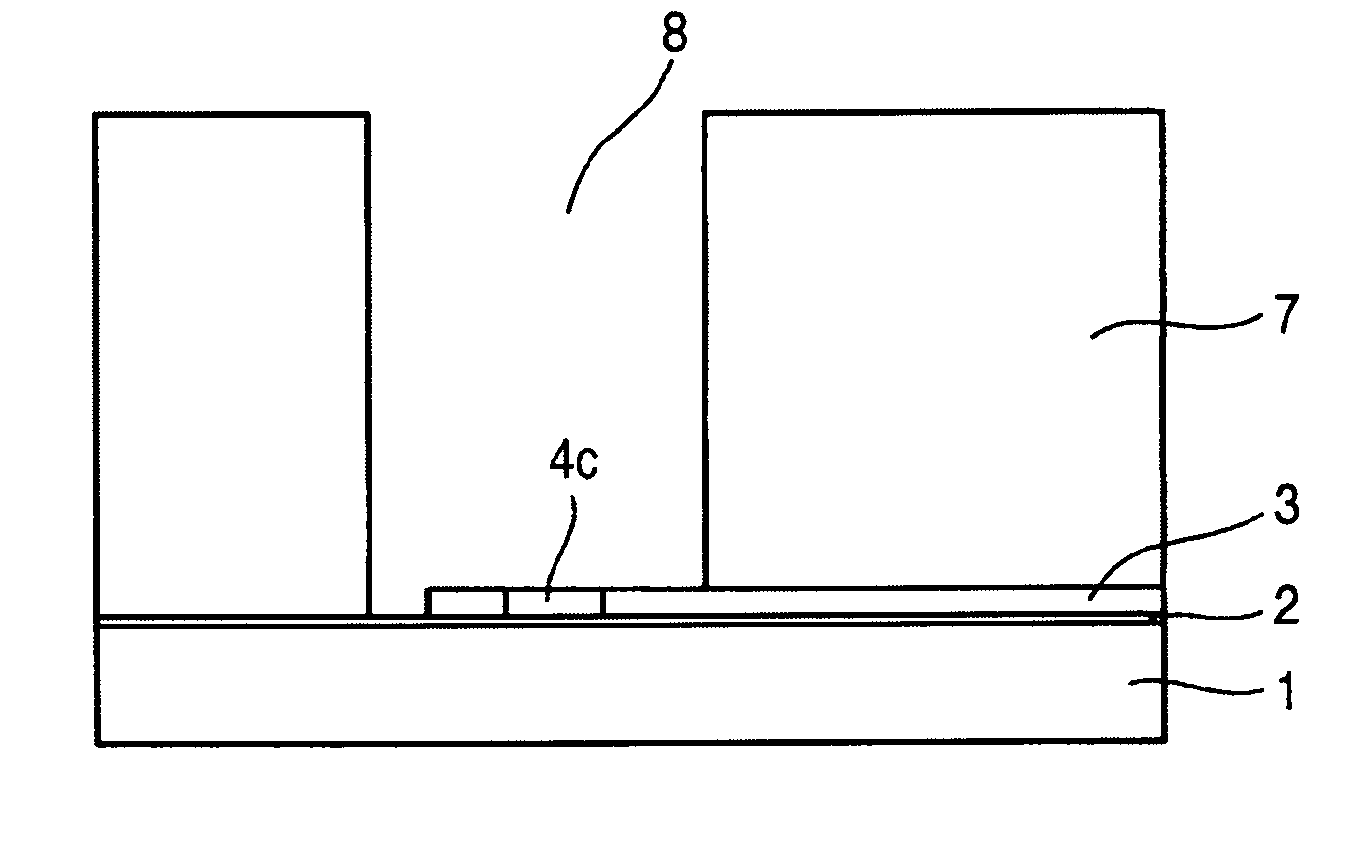
[0040]As shown in FIG. 3(a), the organic insulation layer 1 is formed on a passivasion layer of an integrated circuit on a wafer. The seed layer 2 is formed on the organic insulation layer 1. The wiring 3 is formed on the seed layer 2, and a base portion 4c is disposed in the wiring 3.

[0041]In the second embodiment of the present invention, the base portion 4c functions as a positioning mark for mask matching when the post electrode 5 is formed with photolithography. To this end, as shown in FIG. 3(b), the base portion 4c has a cross shape, which is different from the shape of the base portion 4b shown in FIG. 1(b).

[0042]A resist 7...


PUM


Abstract

A semiconductor device includes a substrate; a wiring formed on the substrate; a base portion disposed at an end portion of the wiring; and an electrode formed on the base portion. The base portion has a size smaller than that of the electrode, so that the base portion is not shifted out of the electrode.

Description

BACKGROUND OF THE INVENTION AND RELATED ART STATEMENT[0001]The present invention relates to a semiconductor device having a packaged structure, and a method of producing the semiconductor device. In particular, the present invention relates to a semiconductor device called a wafer level Chip Size Package (CSP).[0002]Patent Reference has disclosed technology for producing a semiconductor device of this type. FIGS. 4(a) and 4(b) are schematic views showing a post electrode of a conventional semiconductor device, in which FIG. 4(a) is a side view thereof, and FIG. 4(b) is a plan view thereof.[0003]As shown in FIG. 4(a), an organic insulation layer 1 is formed on a passivasion layer of a wafer having an integrated circuit (not shown) formed thereon. A seed layer 2 is formed over a whole surface of the wafer with sputtering, so that plating current flows in a pattern formed with photolithography when a wiring or a post electrode is plated.[0004]A wiring pattern is formed using resist wit...

Claims


Application Information

Patent Timeline
Patent Type & Authority Patents(United States)
IPC IPC(8): H01L23/48
CPCH01L23/3114H01L24/03H01L24/11H01L23/544H01L2924/01033H01L24/94H01L2223/5442H01L2223/54426H01L2223/54453H01L2224/04042H01L2224/1147H01L2224/13099H01L2224/94H01L2924/01004H01L2924/01013H01L2924/01022H01L2924/01029H01L2924/01047H01L2924/01074H01L2924/01078H01L2924/01079H01L2924/014H01L2924/14H01L2224/0401H01L2224/05555H01L2224/13006H01L2224/05568H01L2224/13005H01L2224/05541H01L2224/05552H01L2224/13027H01L2924/01005H01L2924/01006H01L2924/01024H01L2224/11H01L2224/03H01L2924/207H01L2924/00014H01L2924/00012
Inventor OOSUMI, TAKASHI
Owner LAPIS SEMICON CO LTD
Why Eureka
Try Eureka