Physical quantity detecting apparatus and method for driving the same

a technology of physical quantity and detecting apparatus, which is applied in the direction of instruments, television systems, and details of the television system, to achieve the effect of improving bit accuracy and lowering the frequency of the clock signal

Active Publication Date: 2010-03-02
PANASONIC SEMICON SOLUTIONS CO LTD
View PDF9 Cites 32 Cited by
  • Summary
  • Abstract
  • Description
  • Claims
  • Application Information

AI Technical Summary

Benefits of technology

[0034]In Conventional Example 1 shown in FIG. 16, employment of the Gray code expression reduces the necessary switching rate (frequency) to one half of that in the case where the binary expression is employed.
[0036]An object of the invention is providing a solid state imaging device capable of high speed processing with high picture quality even when the number of pixels, the frame rate, the conversion bit width or the like is increased.
[0037]In order to achieve the object, the present inventors have made various examinations, resulting in finding the following: latches are provided in each AD conversion circuit so as to hold clock signals or a value obtained by converting the clock signals into a Gray code or a phase shift code, and thus, lower bits of an AD converted value are expressed. In this manner, the bit width of the AD converted value can be increased without increasing the maximum frequency of the clock signals and without changing conversion time. Alternatively, in the case where the bit width of the AD converted value is not increased, the maximum frequency of the clock signals can be lowered. In particular, when the value held by the latches is expressed by using a Gray code or a phase shift code, the Hamming distance can be always suppressed to the minimum value of “1”, and hence, even when there is skew between bits, the influence of a sampling error can be minimized. Furthermore, since change in a current consumed by counter value change is small, occurrence of noise can be suppressed, and the power consumption can be reduced as compared with the case where a binary code is used. In particular, when a phase shift code is used, the bit accuracy can be improved at the same frequency of a clock signal and the same processing time.
[0039]Owing to the aforementioned architecture, a part of bits of the A / D converted value (lower bits in particular) can be held by the latches. Therefore, the maximum frequency of the counter clock signal to be supplied to the column counter can be lowered. Alternatively, when the frequency and the processing time are the same, bit accuracy can be largely improved as compared with that attained in a conventional physical quantity detecting apparatus. The latch clock signal(s) to be held by the latch(es) may be expressed by using a binary code, a Gray code or a phase shift code, and a Gray code or a phase shift code is preferably used. Particularly, a phase shift code is more preferably used because the bit accuracy of the AD conversion can be thus largely improved without changing the frequency of the counter clock signal and the latch clock signal.
[0041]In this method, the signal read from each of the sensitive elements is AD converted by combining the counter value held by the column counter and the latch clock signal held by the latches (or a value obtained by converting the latch clock signal into a phase shift code or a Gray code). Therefore, the frequency of the clock signal can be lowered while retaining the bit accuracy of the AD conversion. Alternatively, the bit accuracy can be improved while retaining the frequency of the clock signal at a given value.

Problems solved by technology

However, in the case where pixels of, for example, one row are subjected to the AD conversion in parallel as in an AD conversion circuit included in a MOS sensor, it cannot be confirmed whether or not the conversion has been completed with respect to all the pixels by a general architecture, and therefore, the comparison should be performed 1024 times after all.

Method used


Image

  • Physical quantity detecting apparatus and method for driving the same
  • Physical quantity detecting apparatus and method for driving the same
  • Physical quantity detecting apparatus and method for driving the same

Examples


embodiment 1

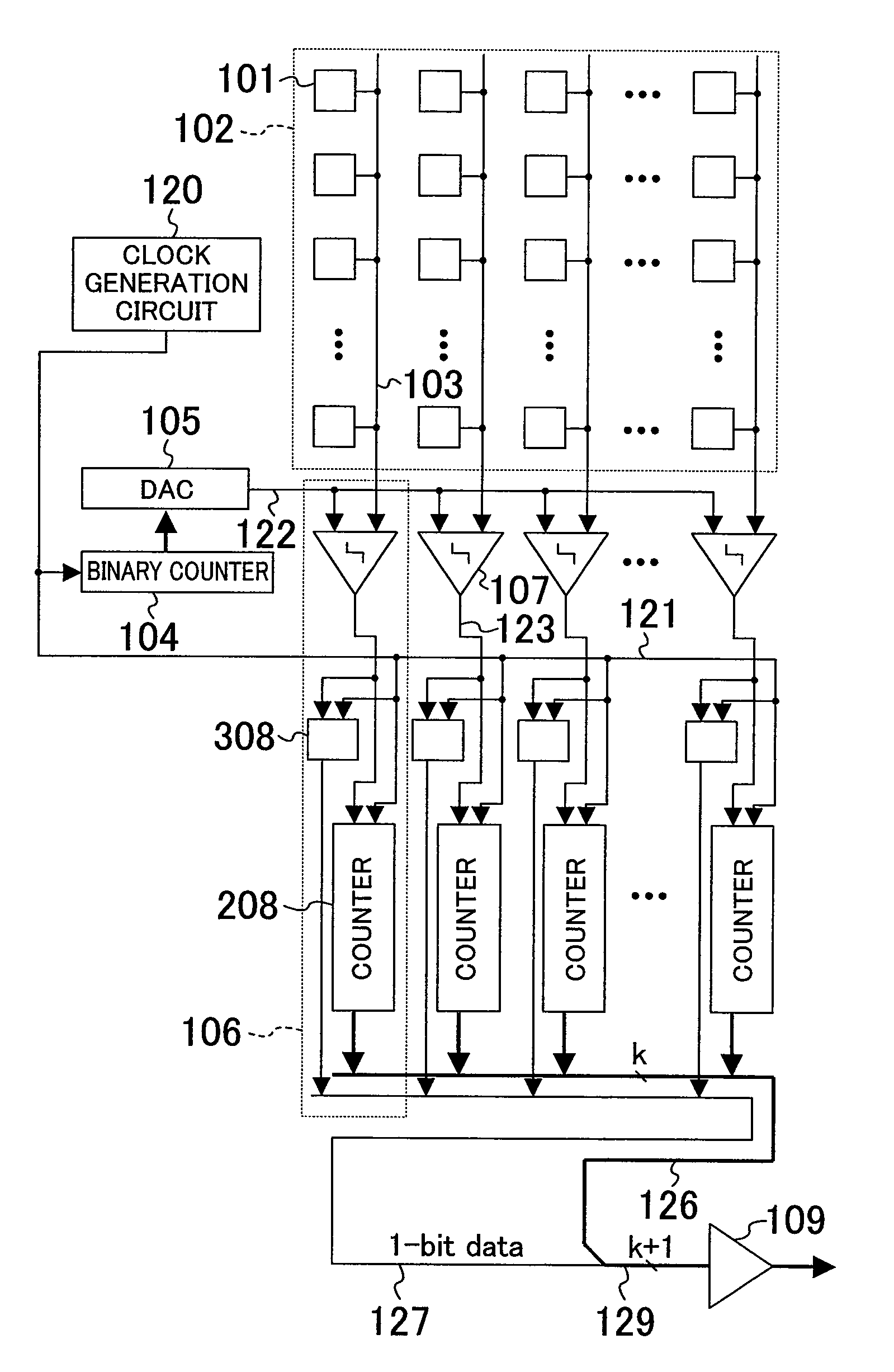
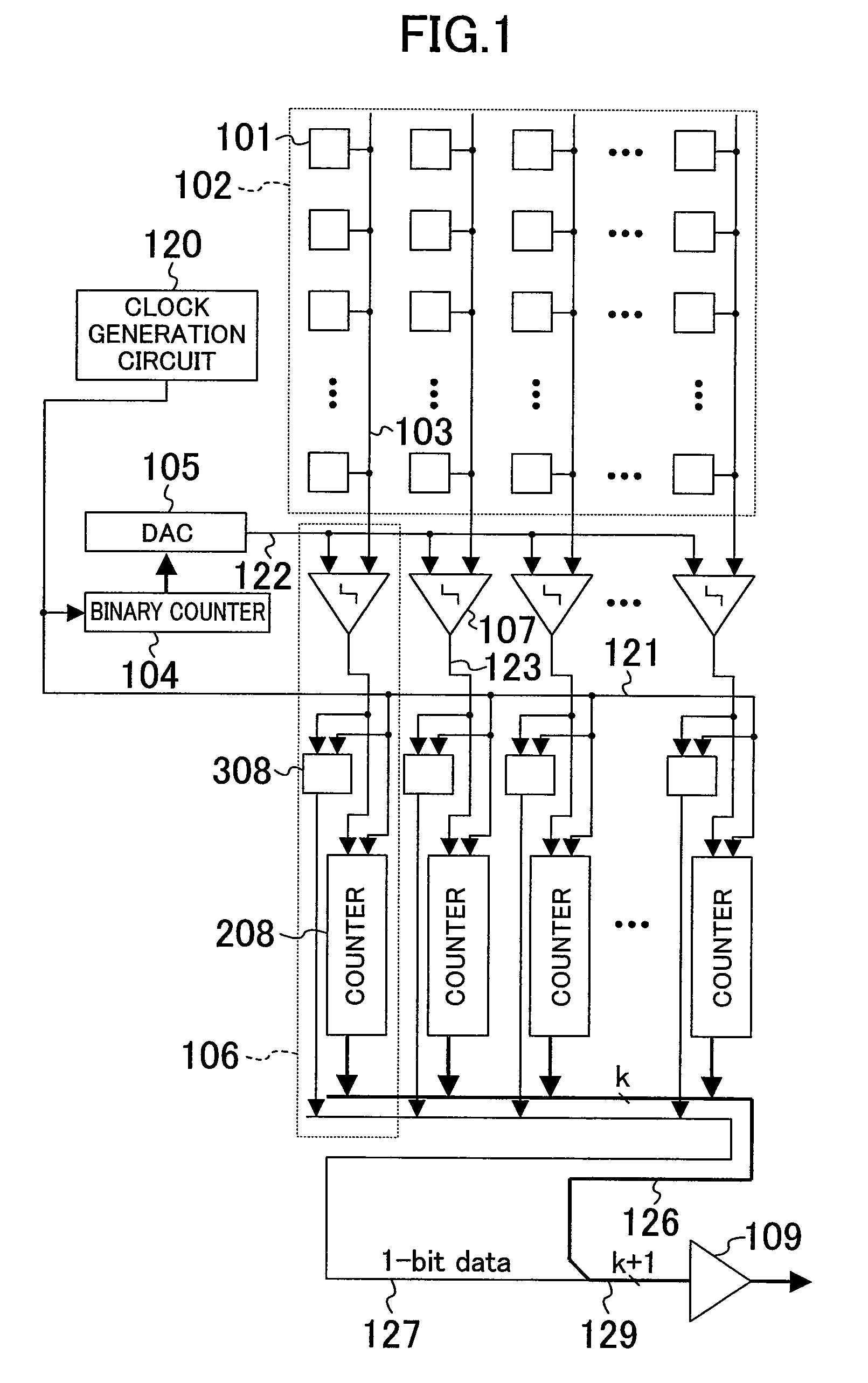
[0073]FIG. 1 is a diagram for showing the architecture of a solid state imaging device (a MOS sensor) according to Embodiment 1 of the invention.

[0074]As shown in FIG. 1, the MOS sensor of this embodiment includes a pixel array (a sensitive element array) 102 in which pixels (sensitive elements) 101 are arranged in the form of a matrix; a column AD conversion circuit 106 provided corresponding to each column or a plurality of columns of pixels 101 for converting a signal output from a pixel 101 into a digital signal; a column scanning circuit (not shown) for controlling output of a digital signal converted and held by the column AD conversion circuit 106; output signal buses 126 and 127 for transferring the digital signal output from the column AD conversion circuit 106; a clock generation circuit 120 for supplying clock signals (including a counter clock signal and a latch clock signal); a binary counter 104; a DA conversion circuit (DAC; a reference potential generation circuit) 1...

embodiment 2

[0094]FIG. 5 is a diagram for showing the architecture of a MOS sensor according to Embodiment 2 of the invention. In FIG. 5, like reference numerals are used to refer to like circuits and members included in the MOS sensor of Embodiment 1 shown in FIG. 1 so as to omit or simplify the description.

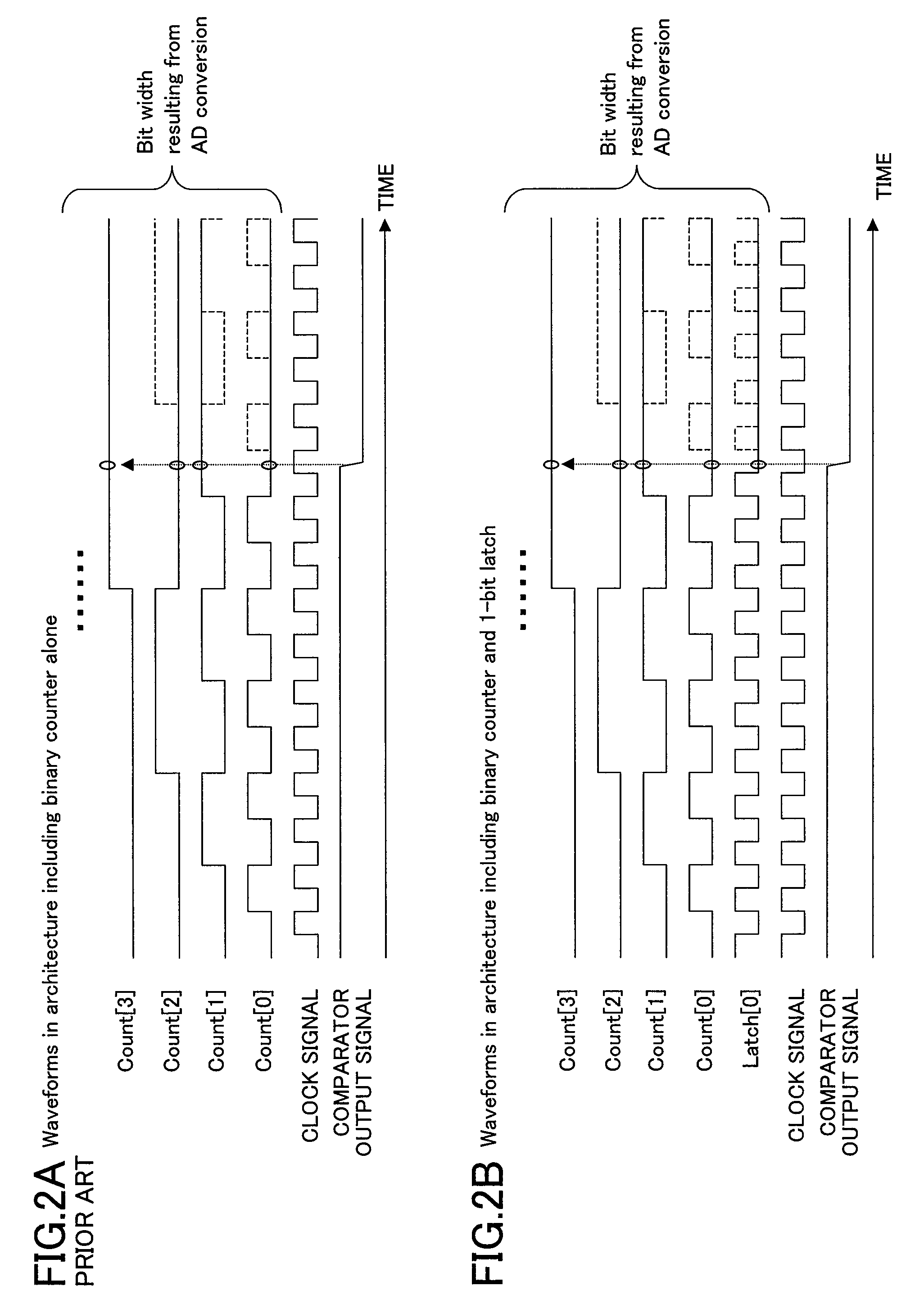
[0095]As shown in FIG. 5, the MOS sensor of this embodiment is the same as the MOS sensor of Embodiment 1 in the connection from a pixel array 102 to comparators 107. However, each column AD conversion circuit 106 of this MOS sensor is different from the column AD conversion circuit of Embodiment 1 in including not only the comparator 107 and a column counter 208 but also a 2m-1-bit latch 408. The column AD conversion circuit 106 is provided corresponding to each column in FIG. 5.

[0096]The MOS sensor of this embodiment further includes a π / 2m-1 phase shift code generation circuit 112 for receiving a clock signal 121 and a phase shift code / binary converter 113 provided on an output signal bu...

embodiment 3

[0119]FIG. 7 is a diagram for showing the architecture of a MOS sensor according to Embodiment 3 of the invention.

[0120]As shown in FIG. 7, the MOS sensor of this embodiment is the same as the MOS sensor of Embodiment 1 in the connection from a pixel array 102 to comparators. However, as a characteristic of the MOS sensor of this embodiment, a column AD conversion circuit 106 provided corresponding to each column of pixels 101 includes an up / down counter (hereinafter referred to as the U / D counter) 218. Also, the MOS sensor of this embodiment includes a sequencer 111.

[0121]Each column AD conversion circuit 106 includes a comparator 107, the U / D counter 218, an up-counting latch (hereinafter referred to as the U latch) 318 and a down-counting latch (hereinafter referred to as the D latch) 328.

[0122]A clock generation circuit 120 supplies a clock signal 121 not only to a binary counter 104 but also to the U / D counter 218, the U latch 318 and the D latch 328 of every column. A binary v...


PUM


Abstract

In a solid state imaging device to be included in an imaging device such as a digital camera, a ramp run-up AD conversion circuit for AD converting a pixel signal is provided corresponding to one or a plurality of pixel columns. A column counter provided in each ramp run-up AD conversion circuit holds an upper bit, and a clock signal is supplied to one or plural latches for holding a lower bit. Thus, fast and accurate AD conversion can be realized while suppressing increase of clock frequency.

Description

BACKGROUND OF THE INVENTION[0001]The present invention relates to a two-dimensional physical quantity detecting apparatus for detecting a physical quantity distribution of electromagnetic waves including visible or invisible light, particle radiations such as alpha rays or beta rays, and more particularly, it relates to a solid state imaging device and a solid state imaging system including sensing elements such as photoelectric conversion elements arranged in the form of a matrix and an AD conversion circuit for receiving an output signal from the sensing elements.[0002]In addition to a CCD (charge coupled device) type sensor (hereinafter referred to as a “CCD sensor”) conventionally mainly used as an image sensor, a MOS type image sensor (hereinafter referred to as a “MOS sensor”) utilizing standard process technology for a logic LSI is widely commercially available in these days. As a characteristic of a MOS sensor, a variety of analog circuits and digital circuits can be integra...

Claims


Application Information

Patent Timeline
Patent Type & Authority Patents(United States)
IPC IPC(8): H04N5/335H04N5/357H04N5/374H04N5/376H04N5/378
CPCH04N5/3742H04N5/378H04N25/767H04N25/75
Inventor SHIMOMURA, KENICHIWATANABE, KENJIABE, YUTAKA
Owner PANASONIC SEMICON SOLUTIONS CO LTD
Why Eureka
Try Eureka