Semiconductor device and method of manufacturing the same
a technology of semiconductor devices and shielding elements, which is applied in the direction of semiconductor devices, electrical equipment, transistors, etc., can solve the problems of inability to cope with surge protection elements around the pad, inability to absorb surge current, and uneven breakdown of chips, so as to prevent current concentration and reduce manufacturing costs. , the current capacity of the protection element can be improved
- Summary
- Abstract
- Description
- Claims
- Application Information
AI Technical Summary
Benefits of technology
Problems solved by technology
Method used
Image
Examples
first embodiment
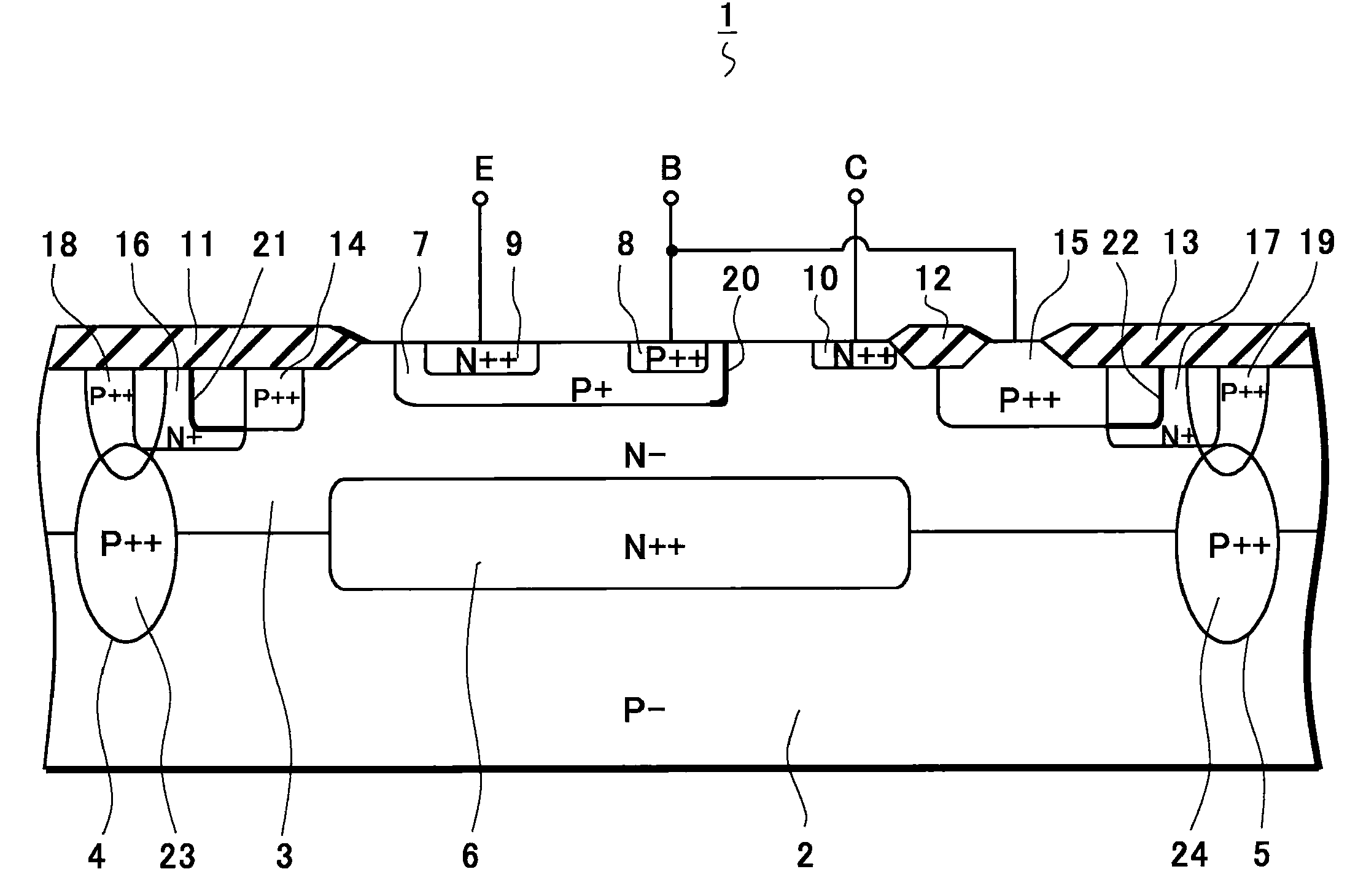
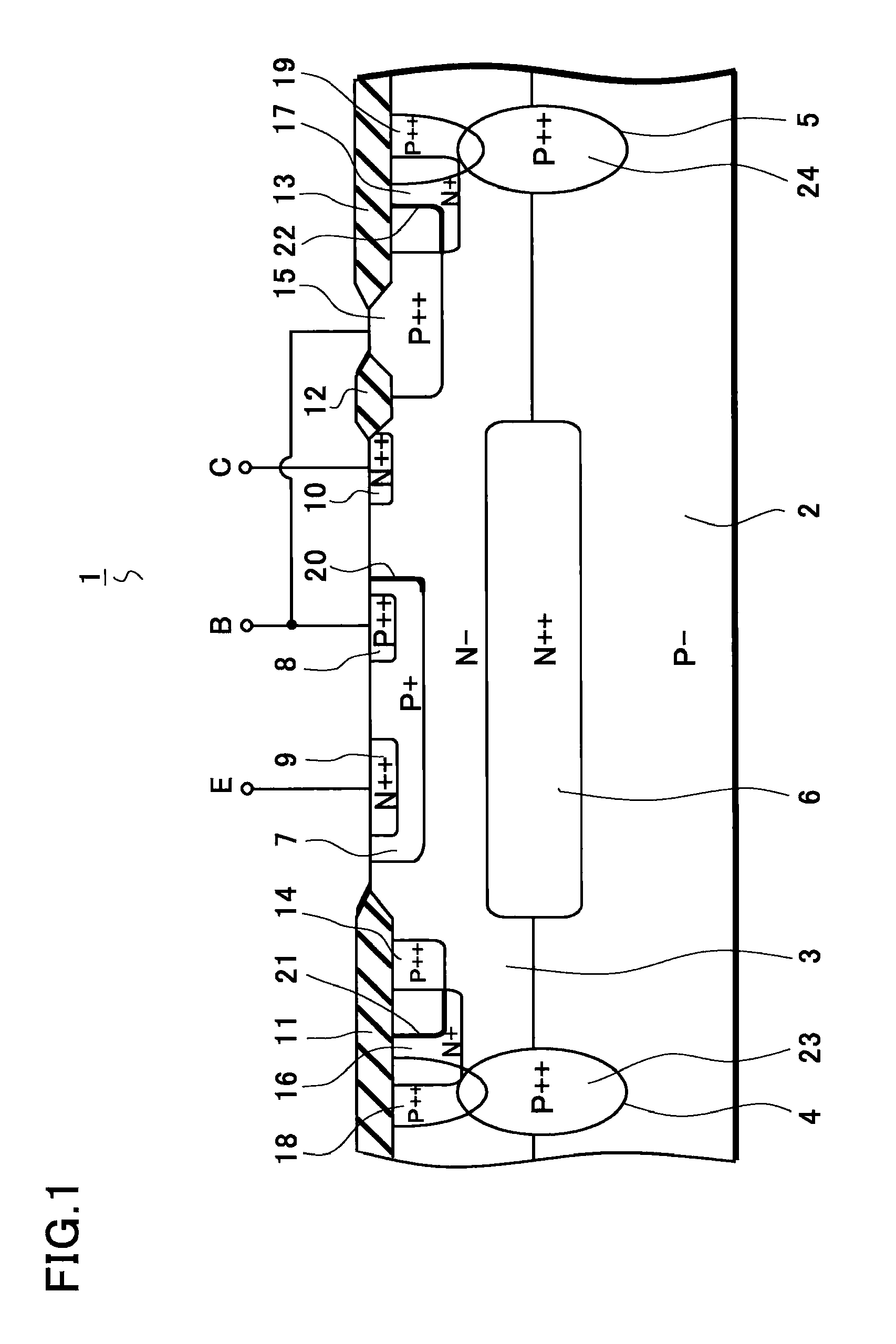
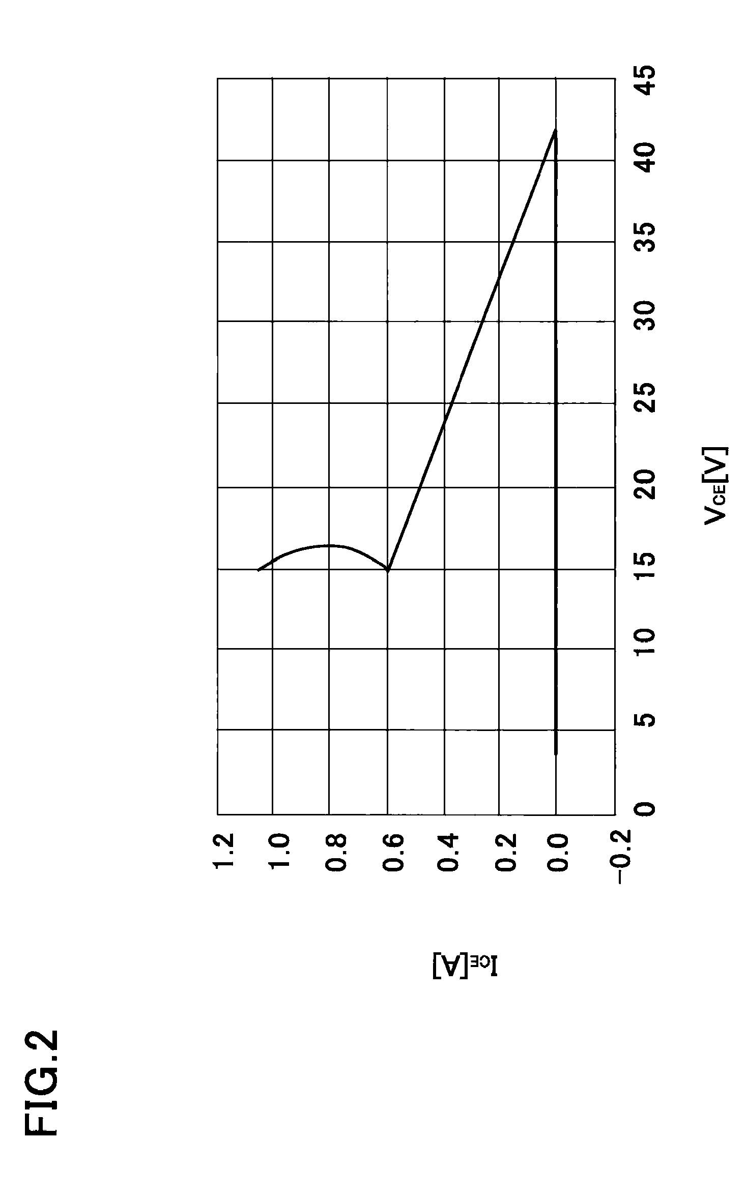
[0036]With reference to FIGS. 1 and 2, a semiconductor device according to the present invention will be described in detail below. FIG. 1 is a cross-sectional view for describing the semiconductor device according to this embodiment. FIG. 2 is a graph for describing characteristics of a protection element in this embodiment.
[0037]As shown in FIG. 1, an NPN transistor 1 mainly includes a P type single crystal silicon substrate 2, an N type epitaxial layer 3, isolation regions 4 and 5, an N type buried diffusion layer 6, P type diffusion layers 7 and 8 used as base regions, an N type diffusion layer 9 used as an emitter region, and an N type diffusion layer 10 used as a collector region.
[0038]The N type epitaxial layer 3 is formed on the P type single crystal silicon substrate 2. Note that, although one epitaxial layer 3 is formed on the substrate 2 in this embodiment, the present invention is not limited to this case. For example, the substrate is stacked with a plurality of epitaxi...
second embodiment
[0071]Next, with reference to FIG. 3, a semiconductor device according to the present invention will be described in detail. FIG. 3 is a cross-sectional view for explaining the semiconductor device according to this embodiment.
[0072]As shown in FIG. 3, a PNP transistor 51 mainly includes a P type single crystal silicon substrate 52, an N type epitaxial layer 53, isolation regions 54 and 55, an N type buried diffusion layer 56, P type diffusion layers 57 and 58 used as collector regions, a P type diffusion layer 59 used as an emitter region, and an N type diffusion layer 60 used as a base lead-out region.
[0073]The N type epitaxial layer 53 is formed on the P type single crystal silicon substrate 52. Note that, although one epitaxial layer 53 is formed on the substrate 52 in this embodiment, the present invention is not limited to this case. For example, the substrate is stacked with a plurality of epitaxial layers.
[0074]Each of the isolation regions 54 and 55 is formed so as to exten...
PUM
 Abstract
Description
Claims
Application Information


