Method of fabricating a wafer structure having a pad and a first protection layer and a second protection layer

a technology of protection layer and wafer, which is applied in the field of wafer structure, can solve the problems of easy cracking, severe tests of heat dissipation and operational stability of semiconductor packages, and jeopardizing the quality of semiconductor packages, so as to improve the yield rate and quality of bonding

Active Publication Date: 2010-03-23
ADVANCED SEMICON ENG INC
View PDF4 Cites 30 Cited by
  • Summary
  • Abstract
  • Description
  • Claims
  • Application Information

AI Technical Summary

Benefits of technology

[0009]The invention is directed to a wafer structure and a method for fabricating the same. At least one material layer in the UBM layer is formed by way of electroplating process, so that the UBM layer can completely cover the wafer, hence improving the yield rate and quality of the bonding between the bump and the pad.

Problems solved by technology

However, due to the miniaturization of volume and size of the products, semiconductor packages are facing severe tests with regard to heat dissipation and operational stability.
The passivation layer is usually relatively thin and susceptible to the stress, and therefore may easily crack.
Under such circumstance, the solder material of the solder layer will contact the electrical pad via the damaged passivation layer and directly jeopardize the quality of semiconductor package.
However, the way of stacking the polymer layer with the passivation layer makes the stacking of the UBM layer at the edges of the polymer layer and the passivation layer even more difficult.
When the UBM layer is sputtered on the electrical pad, the improper stacking may easily occur at the edges of the polymer layer and the passivation layer.
To the worse, the materials of the electrical pad and the solder bump may even spread into one another at the location of improper stacking, making the solder bump brittle or making the metallic material of the electrical pad generate metal void defect.

Method used


Image

  • Method of fabricating a wafer structure having a pad and a first protection layer and a second protection layer
  • Method of fabricating a wafer structure having a pad and a first protection layer and a second protection layer
  • Method of fabricating a wafer structure having a pad and a first protection layer and a second protection layer

Examples


first embodiment

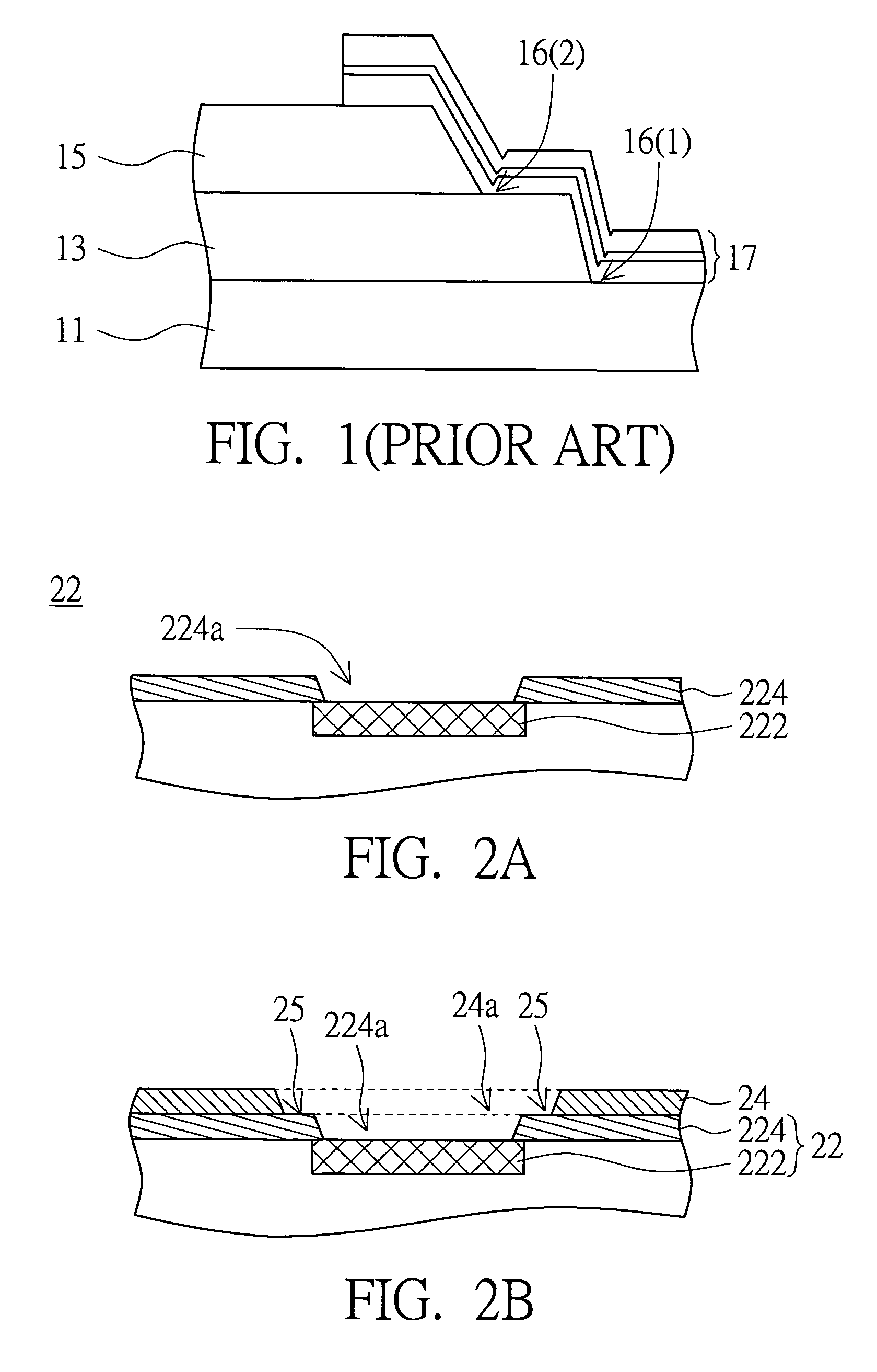
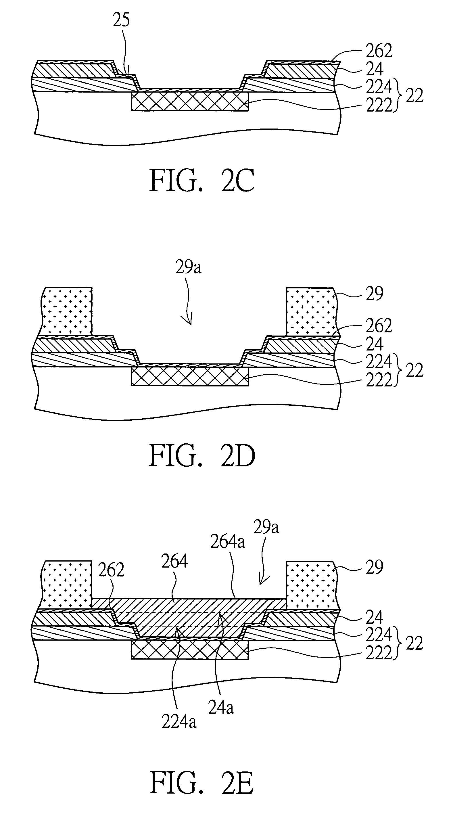
[0039]Please refer to FIG. 2A˜2G at the same time. FIG. 2A is a perspective of a wafer according to a first embodiment of the invention. FIG. 2B is a perspective of a second protection layer formed on the first protection layer in FIG. 2A. FIG. 2C is a perspective of an adhesion layer formed on the wafer and the second protection layer in FIG. 2B. FIG. 2D is a perspective of a photo-resist layer formed on the adhesion layer in FIG. 2C. FIG. 2E is a perspective of a barrier layer electroplated onto the adhesion layer in FIG. 2D. FIG. 2F is a perspective of a wetting layer formed on the barrier layer in FIG. 2E. FIG. 2G is a perspective after the photo-resist layer and part of the adhesion layer in FIG. 2F are removed.

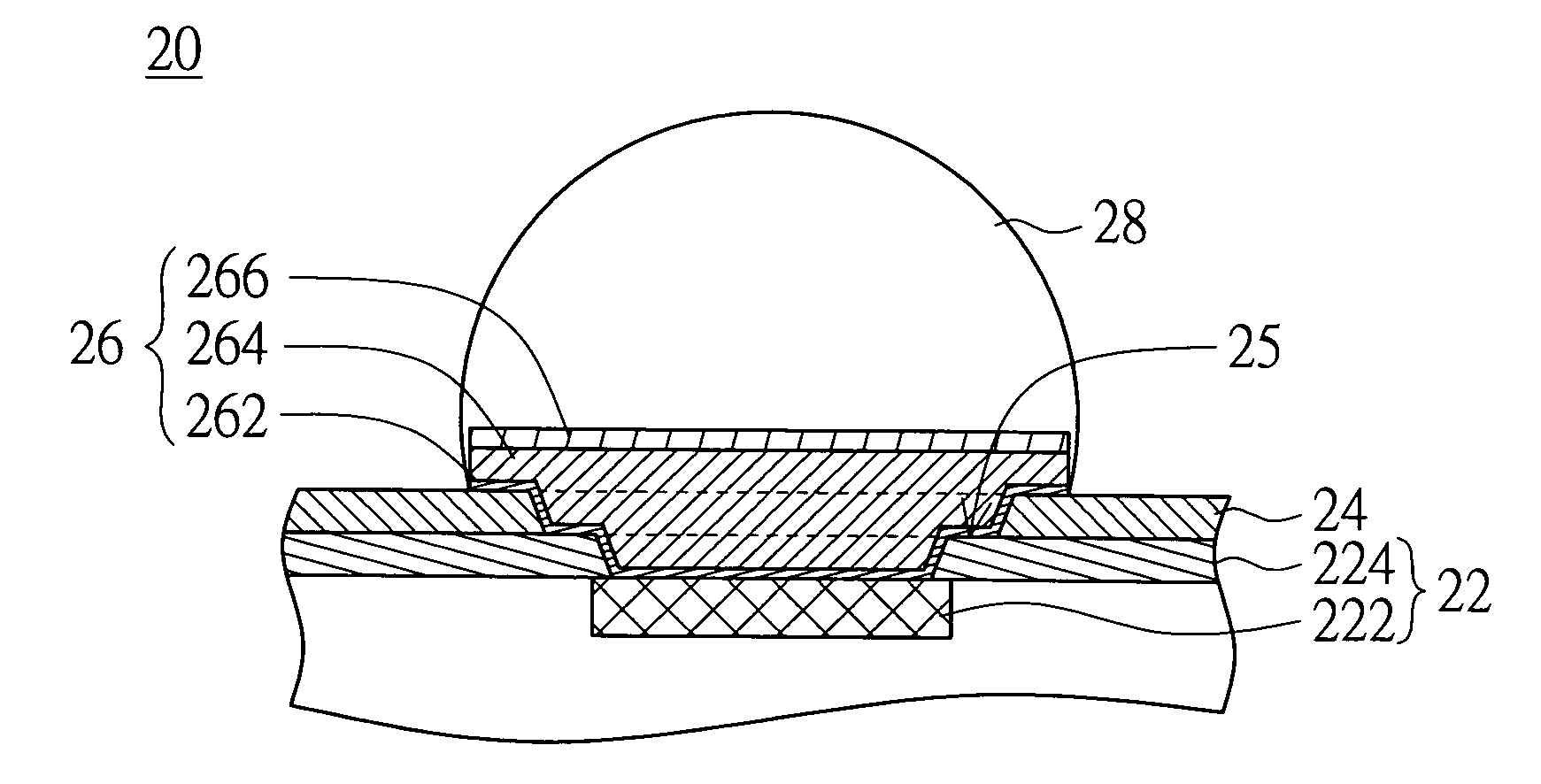
[0040]The method of fabricating a wafer structure according to a first embodiment of the invention includes the following steps. First, a wafer 22 having a pad 222 and a first protection layer 224 is provided. The first protection layer 224 covers the wafer 22 and has a ...

second embodiment

[0050]The present embodiment of the invention differs from the first embodiment in that the T-plug or the U-plug is formed by the wetting layer. Besides that, the method of fabricating wafer structure according to the second embodiment of the invention also sets out from the steps of providing a wafer, forming a second protection layer, forming an adhesion layer and forming a photo-resist layer. These steps are similar to those of the first embodiment, as indicated in FIG. 2A˜2D, and are repeated here.

[0051]Please refer to both FIGS. 4A and 4B. FIG. 4A is a perspective of a barrier layer being formed on the adhesion layer according to a second embodiment of the invention. FIG. 4B is a perspective of a wetting layer being formed on the barrier layer of FIG. 4A. After performing the forming steps mentioned in the above, the fabricating method of the present embodiment of the invention then proceeds to the step of electroplating the barrier layer. As indicated in FIG. 4A, a barrier lay...

third embodiment

[0056]The present embodiment of the invention differs from the first embodiment in the disposition of the photo-resist layer and in the way of forming the UBM layer. Other similarities are not repeated here. Please refer to FIG. 6A˜6G. FIG. 6A is a perspective of a wafer and a second protection layer according to a third embodiment of the invention. FIG. 6B is a perspective of an adhesion layer being formed on the wafer and the second protection layer in FIG. 6A. FIG. 6C is a perspective of a barrier layer being formed on the adhesion layer in FIG. 6B. FIG. 6D is a perspective of a wetting layer being formed on the barrier layer in FIG. 6C. FIG. 6E is a photo-resist layer being formed on the wetting layer in FIG. 6D. FIG. 6F is perspective after the part of the wetting layer, the barrier layer and the adhesion layer exposed outside the photo-resist layer in FIG. 6E are removed. FIG. 6G is a perspective after the photo-resist layer in FIG. 6F.

[0057]The method of fabricating wafer str...


PUM


Abstract

A wafer structure and a method for fabricating the same are provided. First, a wafer having a pad and a first protection layer with a first opening is provided. Next, a second protection layer with a second opening is formed on the first protection layer. Part of the pad and the first protection layer are exposed from the openings. The edges of the openings construct a step structure. Following that, an adhesion layer is formed on the pad, the step structure and the second protection layer. Afterwards, a photo-resist layer with a third opening is formed on the adhesion layer. Then, a barrier layer is electroplated onto part of the adhesion layer. Further, a wetting layer is formed on the barrier layer, and then the photo-resist layer and part of the adhesion layer exposed outside the barrier layer are removed. Finally, a solder layer is printed onto the wetting layer.

Description

[0001]This application claims the benefit of Taiwan application Ser. No. 96119957, filed Jun. 4, 2007, the subject matter of which is incorporated herein by reference.BACKGROUND OF THE INVENTION[0002]1. Field of the Invention[0003]The invention relates in general to a wafer structure and a method for fabricating the same, and more particularly to a wafer structure having an electroplated layer and a method for fabricating the same.[0004]2. Description of the Related Art[0005]As electronic products become more and more popular in the market, more functions are provided into the products to meet consumers' demands. Along with the developing of multifunctional electronic products, more and more semiconductor packages are needed in the products. However, due to the miniaturization of volume and size of the products, semiconductor packages are facing severe tests with regard to heat dissipation and operational stability. Therefore, the quality of semiconductor packages becomes one of the...

Claims


Application Information

Patent Timeline
Patent Type & Authority Patents(United States)
IPC IPC(8): H01L21/44
CPCH01L24/11H01L2224/05568H01L2924/0002H01L2224/05572H01L2224/13099H01L2224/16H01L2924/01013H01L2924/01022H01L2924/01029H01L2924/01047H01L2924/01074H01L2924/01078H01L2924/01079H01L2924/01082H01L2924/01023H01L2924/01024H01L2924/01033H01L2924/014H01L2224/0401H01L2224/05552H01L24/03H01L24/05H01L24/13H01L2224/05124H01L2224/05147H01L2224/05155H01L2224/05166H01L2224/05171H01L2224/05556H01L2224/05644H01L2224/05647H01L2224/05655H01L2924/351H01L2924/00H01L2924/00012H01L2924/00014H01L2924/013
Inventor WEN, SHAU-CHUO
Owner ADVANCED SEMICON ENG INC
Why Eureka
Try Eureka