Semiconductor device manufacturing method

a technology of semiconductor devices and manufacturing methods, applied in the direction of semiconductor devices, basic electric elements, electrical equipment, etc., can solve the problems of difficult to fill the trench with insulating materials, difficult to meet the requirements of the trench, and the aspect ratio of the sti region becomes higher, and achieves less susceptibility

Inactive Publication Date: 2010-03-30
KK TOSHIBA
View PDF32 Cites 7 Cited by
  • Summary
  • Abstract
  • Description
  • Claims
  • Application Information

AI Technical Summary

Benefits of technology

[0012]A semiconductor device manufacturing method according to a second aspect of the present invention comprises forming a second semiconductor layer which has less susceptibility to adopting insulative characteristics than a first semiconductor layer on the first semiconductor layer, forming grooves in the first and second semiconductor layers and form fin-shaped semiconductor structures which are each sandwiched between the grooves, and changing portions of the first and second semiconductor layers which are exposed to the grooves into an insulator form to fill the grooves with the insulator-form portions of the first semiconductor layer, narrow the width of a portion of the first semiconductor layer which lies in each of the fin-shaped semiconductor structures by use of the insulator-form portion of the first semiconductor layer and cause the second semiconductor layer to overhang the insulator-form portion of the first semiconductor layer.

Problems solved by technology

The STI region is advantageous for miniaturization, but some difficult conditions occur when the semiconductor device is further miniaturized.
One of the problems is that the aspect ratio of the STI region becomes higher.
In the STI region with the enhanced aspect ratio or the STI region having the opening diameter reduced, one of the difficult conditions is that it becomes difficult to fill the trench with an insulating material.

Method used


Image

  • Semiconductor device manufacturing method
  • Semiconductor device manufacturing method
  • Semiconductor device manufacturing method

Examples


first embodiment

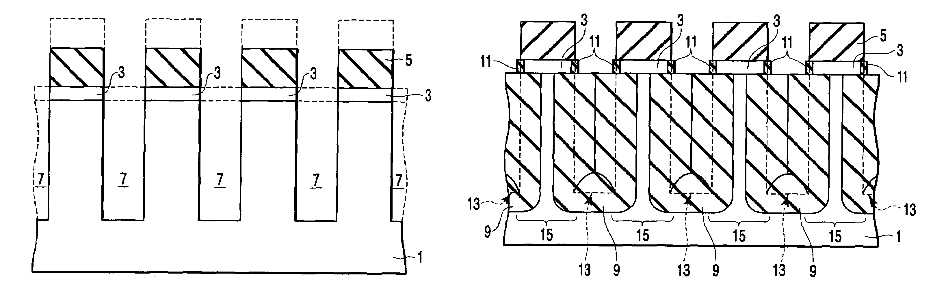
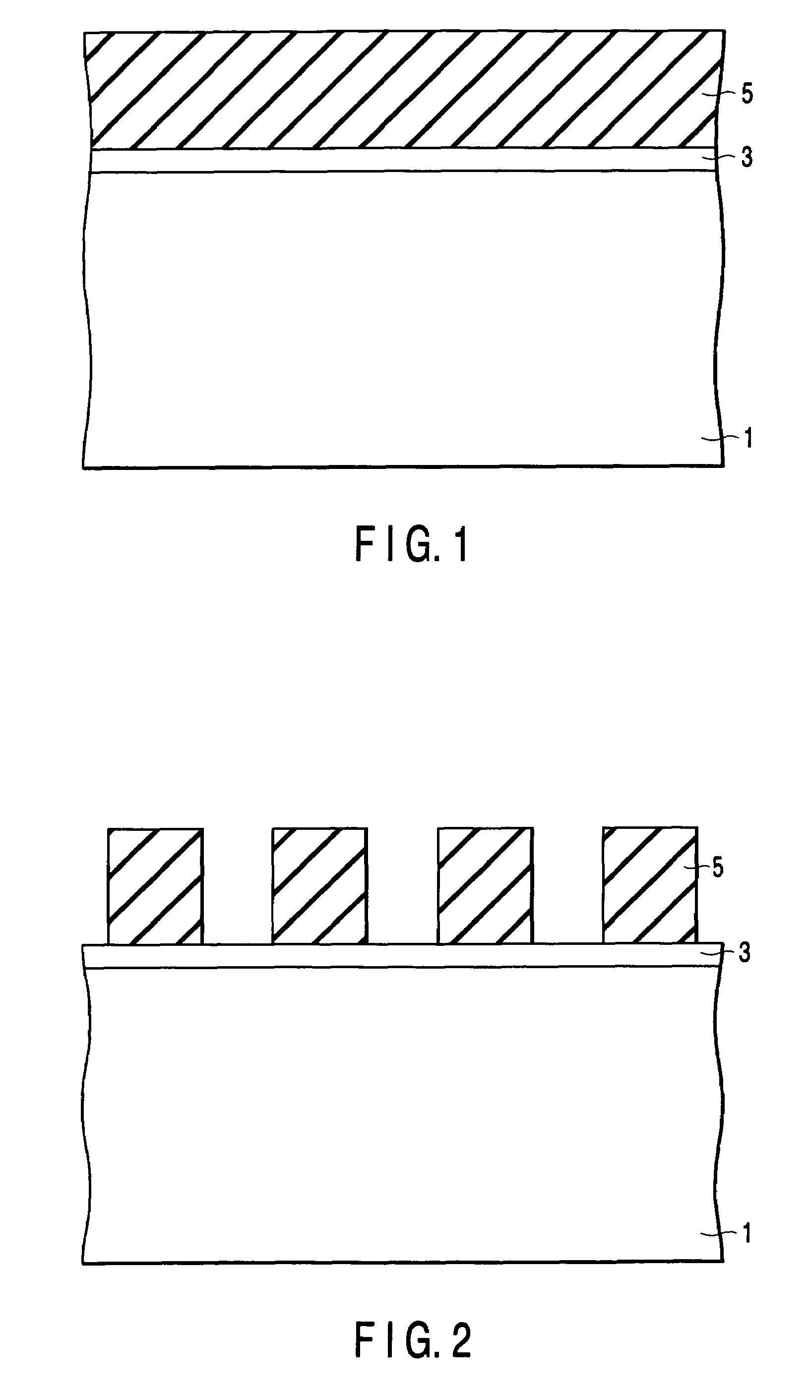
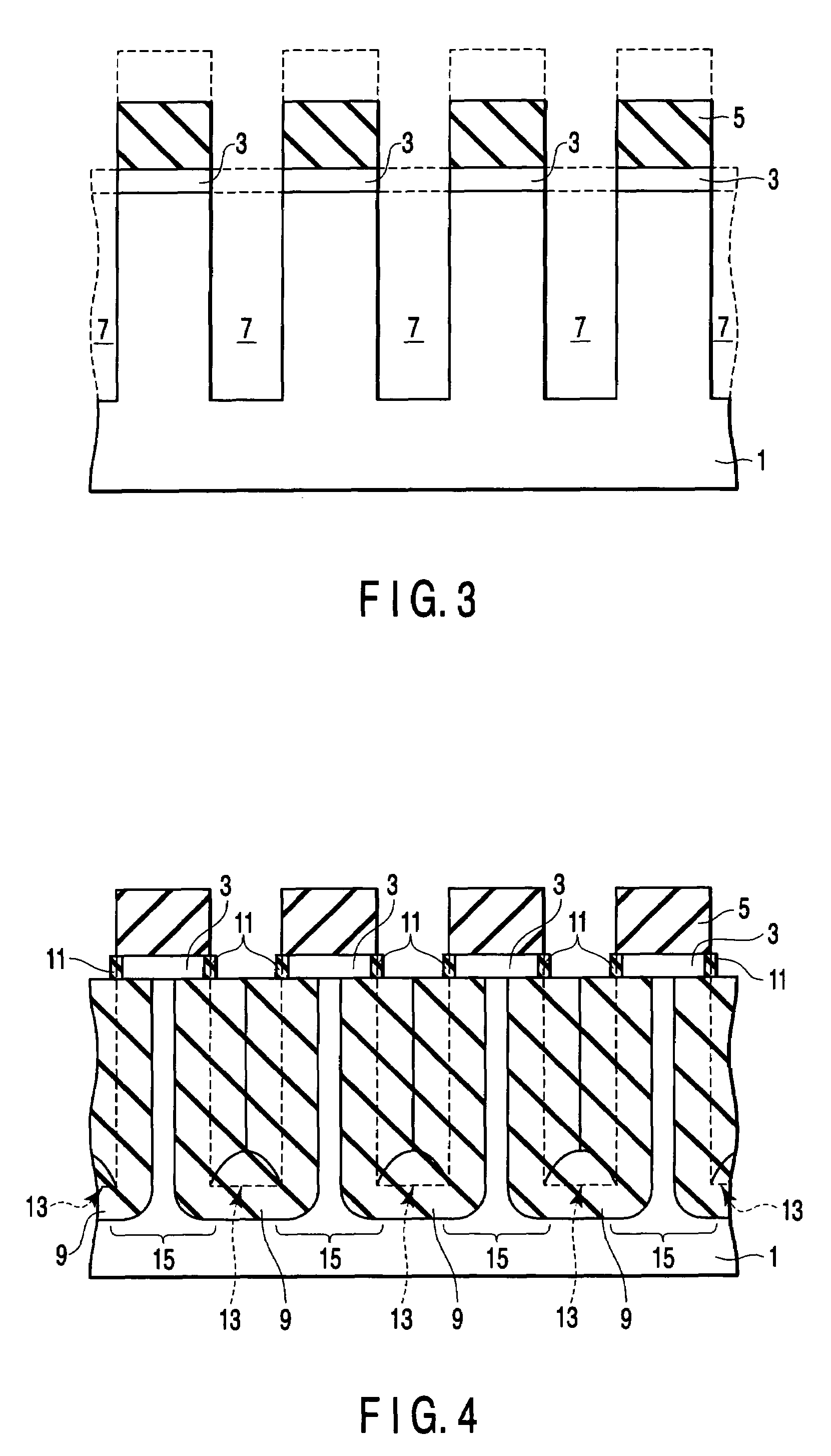
[0059]FIGS. 1 to 4 are cross sectional views showing one example of a semiconductor device manufacturing method according to a first embodiment of this invention.

[0060]As shown in FIG. 1, a second semiconductor layer 3 is formed on a first semiconductor layer 1. One example of the first semiconductor layer is a semiconductor substrate, that is, a semiconductor wafer and one concrete example of the second semiconductor layer 3 is a layer formed with thin film thickness on the surface of the semiconductor substrate or a thin film deposited to thin film thickness on the semiconductor substrate. In this example, the semiconductor material of the second semiconductor layer 3 is selected from semiconductor materials which are more difficult to be changed or modified into an insulator form than the first semiconductor layer 1. One example of the insulation process is oxidation.

[0061]In this example, as a material of the first semiconductor layer 1, a semiconductor material containing two o...

second embodiment

[0094]The second embodiment relates to an example associated with the definition of the width of a trench and relates to a semiconductor device having various widths of trenches.

[0095]FIG. 13 is a cross sectional view showing a first example of the width of a trench and FIG. 14 is a cross sectional view showing a second example of the width of a trench.

[0096]As shown in FIG. 13, the first example of a trench 7 is an example in which the trench 7 can be filled with an SiGe oxide 9 as explained in the first embodiment. In this case, the width “Wt” of the trench 7 is set to “Wt≦(Tsg×2)” when the thickness of the SiGe oxide 9 which grows from the side walls (the original surfaces are indicated by reference symbols 13) of the trench 7 is set to “Tsg”.

[0097]On the other hand, as shown in FIG. 14, when the width “Wt” of the trench 7 is set to “Wt>(Tsg×2)”, the trench 7 cannot be fully filled with the SiGe oxide 9 and a concave portion 61 is formed.

[0098]In a semiconductor integrated circui...

third embodiment

[0102]The third embodiment relates to a semiconductor device obtained by further improving the characteristic of the semiconductor device having the strained semiconductor structure.

[0103]The operation speed of the semiconductor device having the strained semiconductor structure is further enhanced if tensile force is caused in a P-type Si layer 3 in a strained semiconductor N-channel MISFET and compressive force is caused in an N-type Si layer 3 in a strained semiconductor P-channel MISFET. Basically, in the case of the P-type Si layer 3, a tensile material 71 which applies tensile force to the P-type Si layer 3 is formed around the P-type Si layer 3 as shown in FIG. 17. In the case of the N-type Si layer 3, a compression material 73 which applies compressive force to the N-type Si layer 3 is formed around the N-type Si layer 3 as shown in FIG. 18.

[0104]A case wherein, for example, the structure shown in FIG. 17 is applied to the MISFET having the typical STI structure is shown in ...


PUM


Abstract

A semiconductor device manufacturing method is disclosed. The method is to form a second semiconductor layer which has less susceptibility to adopting insulative characteristics than a first semiconductor layer on the first semiconductor layer. Then, grooves which expose portions of the second and first semiconductor layers are formed to extend from the upper surface of the second semiconductor layer into the first semiconductor layer. Next, portions of the first and second semiconductor layers which are exposed to the grooves are changed into an insulator form to fill the grooves with the insulator-form portions of the first semiconductor layer.

Description

CROSS-REFERENCE TO RELATED APPLICATIONS[0001]This application is based upon and claims the benefit of priority from prior Japanese Patent Application No. 2004-181076, filed Jun. 18, 2004, the entire contents of which are incorporated herein by reference.BACKGROUND OF THE INVENTION[0002]1. Field of the Invention[0003]This invention relates to a semiconductor device manufacturing method and more particularly to a manufacturing method of a semiconductor device having fine trench isolation.[0004]2. Description of the Related Art[0005]In recent years, as an element isolation region of a semiconductor device, a shallow trench isolation (STI) region is widely used instead of a local oxidation (LOCal Oxidation of Silicon: LOCOS) type element isolation region. The STI region is less subject to mask conversion errors since the “bird's beak” is not grown, unlike the LOCOS region. Further, in the STI region, the isolation region can be formed deeper and the isolation distance between the adjace...

Claims


Application Information

Patent Timeline
Patent Type & Authority Patents(United States)
IPC IPC(8): H01L21/76H01L21/762H01L21/8238
CPCH01L21/76208H01L29/7842H01L21/823807H01L21/823878
Inventor KAWASAKI, HIROHISAISHIMARU, KAZUNARIKASAI, KUNIHIROOKAYAMA, YASUNORI
Owner KK TOSHIBA
Why Eureka
Try Eureka