Back-lit image sensor with a uniform substrate temperature
a back-lit image sensor and substrate temperature technology, applied in the field of image sensors, can solve the problems of difficult formation, affecting the heat dissipation of image sensors, and affecting the normal path of light rays from each lens to the photodiode of the associated photosensitive cell,
- Summary
- Abstract
- Description
- Claims
- Application Information
AI Technical Summary
Benefits of technology
Problems solved by technology
Method used
Image
Examples
first embodiment
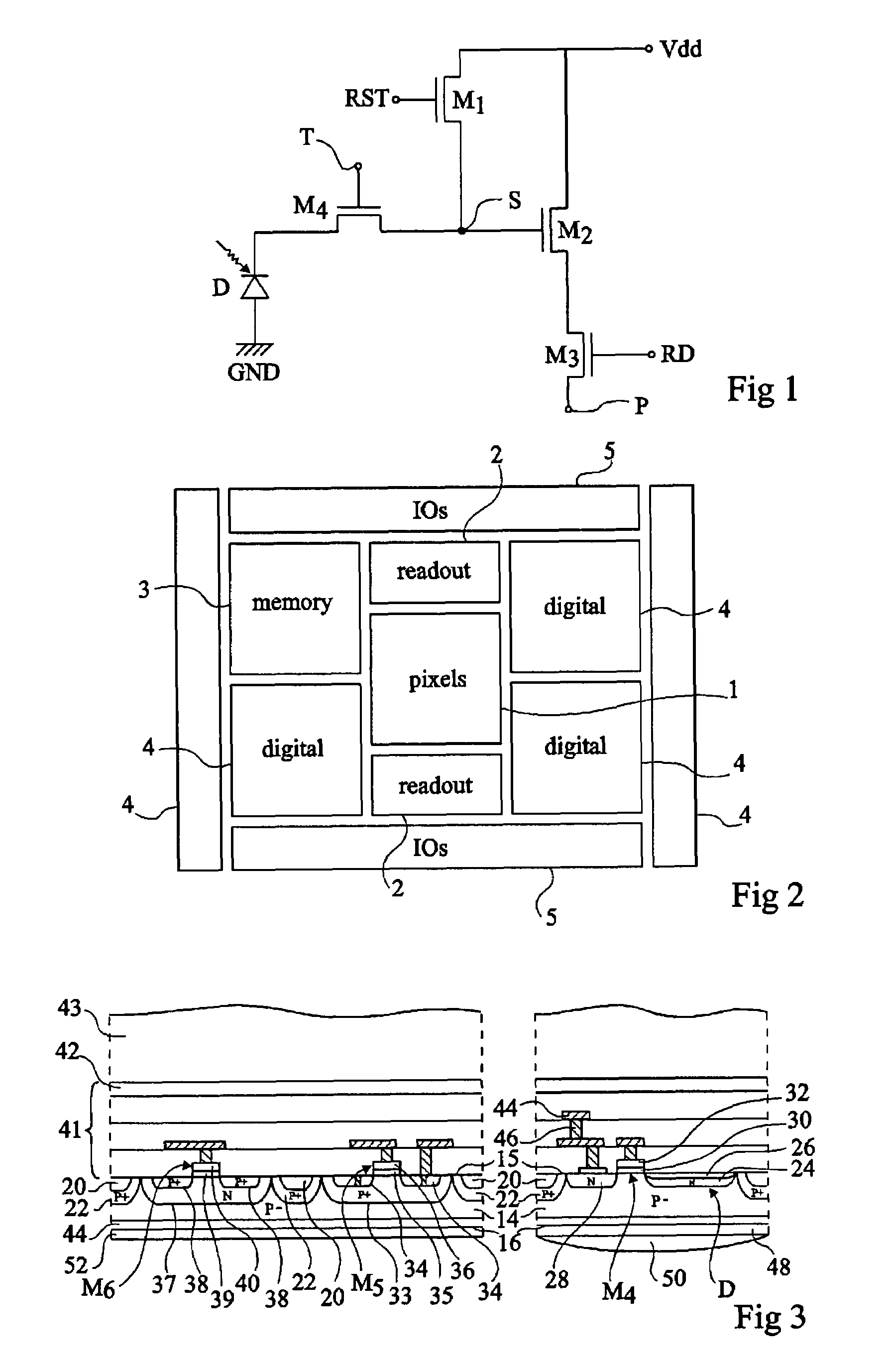
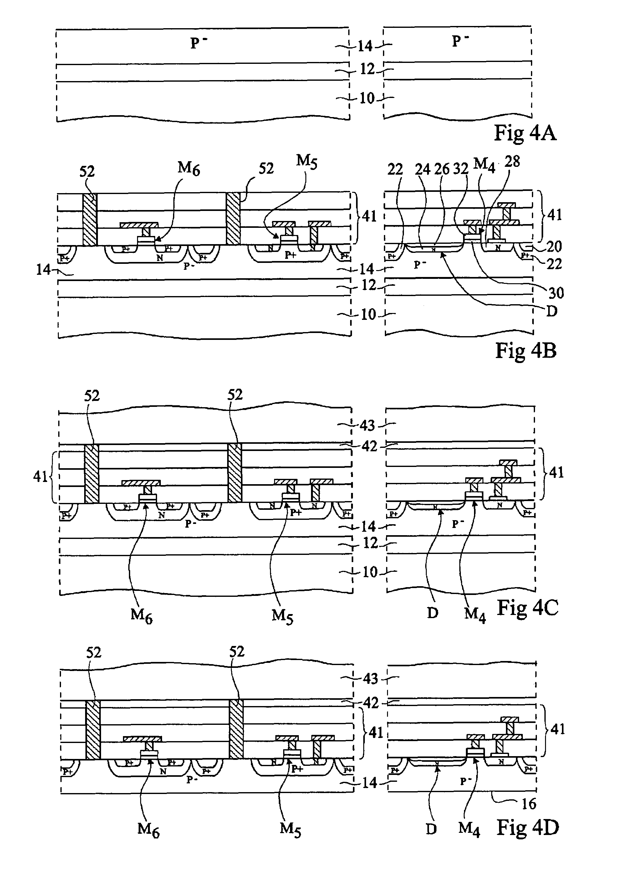
[0038]FIGS. 4A to 4E illustrate an example of a method for manufacturing a back-lit image sensor according to the present invention. The elements common with FIG. 3 have been designated with the same reference numerals.
[0039]FIG. 4A shows a solid silicon support 10 covered with an insulating layer 12, for example, a thermal oxide. Substrate 14 is formed on insulating layer 12 with the possible interposition of a seed layer. Substrate 14 has a thickness of a few micrometers, preferably lower than 5 μm. Such a structure corresponds to an SOI structure (silicon on insulator).
[0040]FIG. 4B shows the structure obtained after having formed all the electronic components of the photosensitive cells and of the peripheral circuits, as well as stack 41 of insulating layers, metal tracks 44, and vias 46. For each photosensitive cell, although only photodiode D and transistor M4 are shown in FIG. 4B, the other cell transistors, that is, transistors M1, M2, and M3, are also formed at the level of...
second embodiment
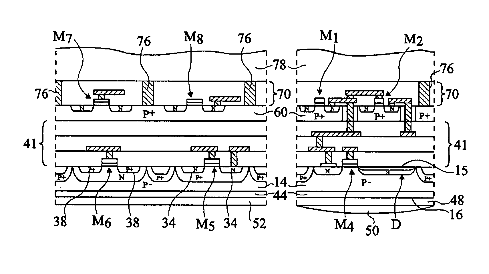
[0045]FIGS. 5A to 5F illustrate the steps of an example of a method for manufacturing a back-lit image sensor according to the present invention.
[0046]FIG. 5A illustrates the structure obtained after steps similar to those which have been previously described for the method for manufacturing the first embodiment of the image sensor according to the present invention in relation with FIGS. 4A and 4B. However, conversely to what has been previously described, only photodiode D and transfer transistor M4 are formed for each photosensitive cell. As to the peripheral circuits, only the components which do not exhibit a significant heat dissipation are formed. Further, vias 52 are not formed. Moreover, vias 58 which extend to the upper surface of stack 41 of insulating layers are provided.
[0047]FIG. 5B shows the structure obtained after having formed on the stack of insulating layers 41 a P-type single-crystal silicon layer 60, possibly more heavily doped than substrate 14. The thickness ...
PUM
 Abstract
Description
Claims
Application Information


