High frequency circuit board converting a transmission mode of high frequency signals

a transmission mode and high frequency technology, applied in the field of high frequency circuit boards, can solve the problems of inefficiency in the conversion of transmission modes, the difficulty of creating them in the case of organic substrates, and the increase of the gap, so as to suppress the generation of parallel plate modes and enhance isolation. the effect of low loss

Inactive Publication Date: 2010-03-30
DENSO CORP
View PDF7 Cites 2 Cited by
  • Summary
  • Abstract
  • Description
  • Claims
  • Application Information

AI Technical Summary

Benefits of technology

[0011]Accordingly, an object of the present invention is to realize conversion of a transmission mode from a microstrip line to a coplanar line efficiently and with low loss.
[0012]This enables realizing a high frequency circuit board which is capable of inputting and outputting signals to a semiconductor device with low loss and low reflection loss.
[0016]The transmission mode coverts in three stages: the microstrip line, the first coplanar line portion, and the second coplanar line portion, which enables efficient conversion of a transmission mode from the microstrip line to the coplanar line with low loss, without any sharp change in the transmission mode from the microstrip line to the coplanar line.
[0017]The first signal strip conductor and the second signal strip conductor may be connected to each other with a wire or the like to match impedance. If impedance is matched, the first signal strip conductor and the second signal strip conductor may have a continued configuration. In addition, since the first aspect of the present invention realizes conversion of a transmission mode with a two-layer configuration as described above, it is possible to increase a gap between the signal line and the ground line to, for example, approx. 100 μm. Hence, an organic substrate with a reduced production cost can be used as a circuit board.
[0023]The shape with gradually decreased or increased width of the conductor generates an evanescent wave which serves as capacitance, which causes phase rotation to increase. In addition, the shape of the second ground strip conductor causes current to converge to the wire at once, thereby generating an evanescent wave. The evanescent wave serves as an inductor, which causes phase rotation to increase. The effect of the two phase rotations as described above enables shortening the line length of the coplanar line. Particularly, as in the sixth aspect of the present invention, the shape with gradually decreased or increased width of the conductor is a fan shape at least at an end portion region is capable of further increasing capacitance and inductor caused by the evanescent wave, enabling further shortening the line length.
[0025]In the first aspect of the present invention, the dielectric region is interposed between the second signal strip conductor and the first ground strip conductor. In addition, the first aspect of the present invention realizes a transmission mode which is a transmission mode of a quality between the transmission mode for the microstrip line and the transmission mode for the coplanar line by having a two-layered structure, and converts the transmission mode from the microstrip line to the coplanar line in a phased manner. Accordingly, the first aspect of the present invention enables conversion of a transmission mode with low loss. Furthermore, as in the second and third aspects of the present invention, when the coplanar line and the semiconductor device are connected to each other, the ground closer to the semiconductor device can be made imaginary ground, which enables suppressing generation of the parallel plate mode. The second and third aspects of the present invention also enable enhancing isolation between other ports. In addition, as in the fourth, fifth and sixth aspects of the present invention, use of a shape with gradually decreased or increased width of the conductor enables shortening the length of conversion from the microstrip line to the coplanar line, thereby enabling minituraization. In addition, the high frequency circuit board according to the present invention, as in the seventh aspect of the present invention, can also be used in a millimeter waveband. Moreover, the present invention does not require microfabrication and enables increasing the gap between the signal line and the ground line to, for example, approx. 100 μm, which enables use of an organic substrate thereby enabling reducing the cost.

Problems solved by technology

However, since the gap between the signal line of the coplanar line and the ground line is only approx.
20 μm even at the narrowest portion, it is very difficult to create it in the case where an organic substrate is used.
Specifically, in the case where an organic substrate is used to decrease the manufacturing cost, the gap which can be created increases.
As a result of this, according to the conversion method as described in the Japanese Patent Laid-open Publication No. 2001-94012 and Japanese Patent Laid-open Publication No. 2001-102820, conversion of a transmission mode cannot be performed efficiently, and it is difficult to connect the wire to the line of the semiconductor while the transmission mode for the coplanar line remains unchanged.
S64-5102, conversion of a transmission mode from the microstrip line to the coplanar line occurs rapidly, and thereby increasing a loss.

Method used


Image

  • High frequency circuit board converting a transmission mode of high frequency signals
  • High frequency circuit board converting a transmission mode of high frequency signals
  • High frequency circuit board converting a transmission mode of high frequency signals

Examples


first embodiment

[0039]First, a configuration of a high frequency circuit board according to the present invention will be described.

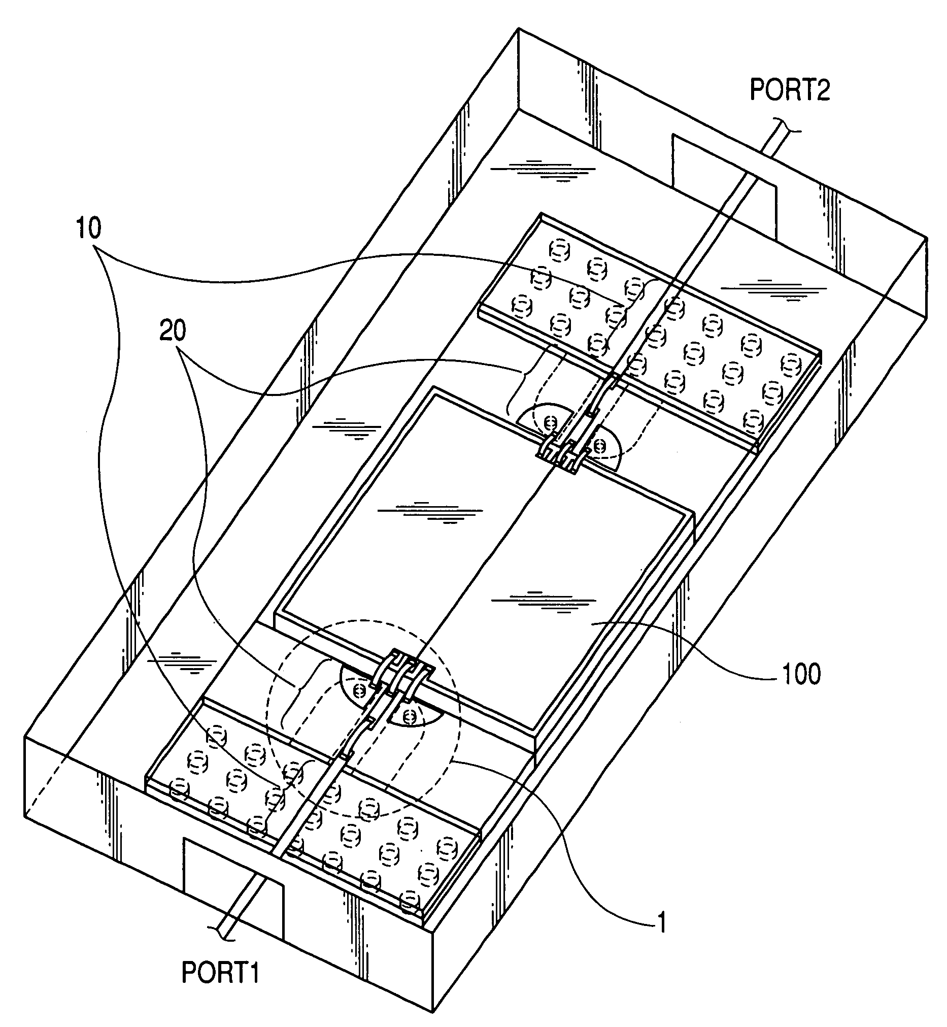
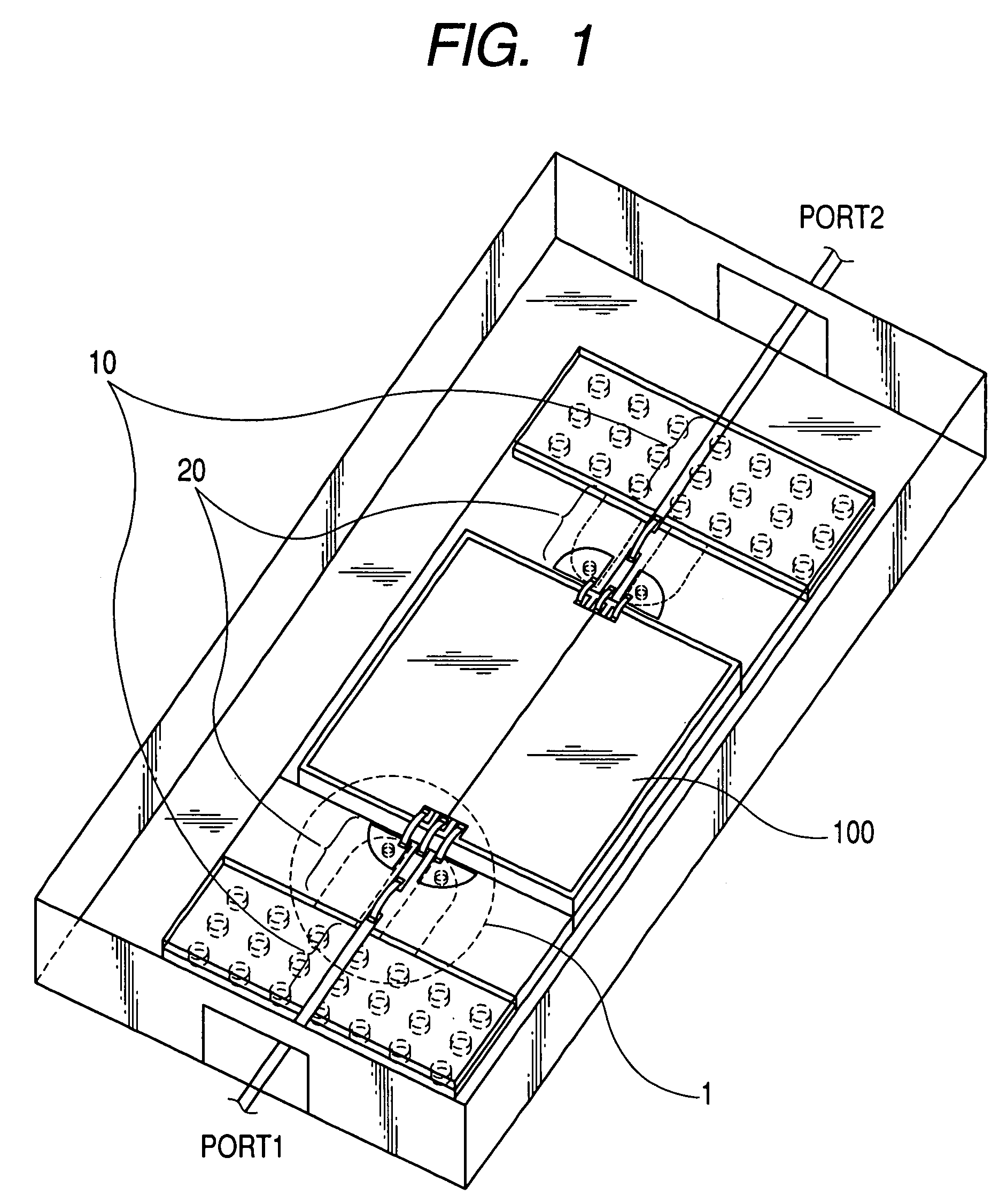
[0040]FIG. 1 is a view of high frequency circuit board according to the present invention seen from diagonally above. The high frequency circuit board includes a microstrip line 10, a coplanar line 20, and ports 1, 2, and is symmetrically configured laterally and vertically. The high frequency circuit board is also mounted with a chip 100. In this case, because of ease of simulation, in place of a semiconductor device, a dummy chip 100 formed with a microstrip line 105 is used.

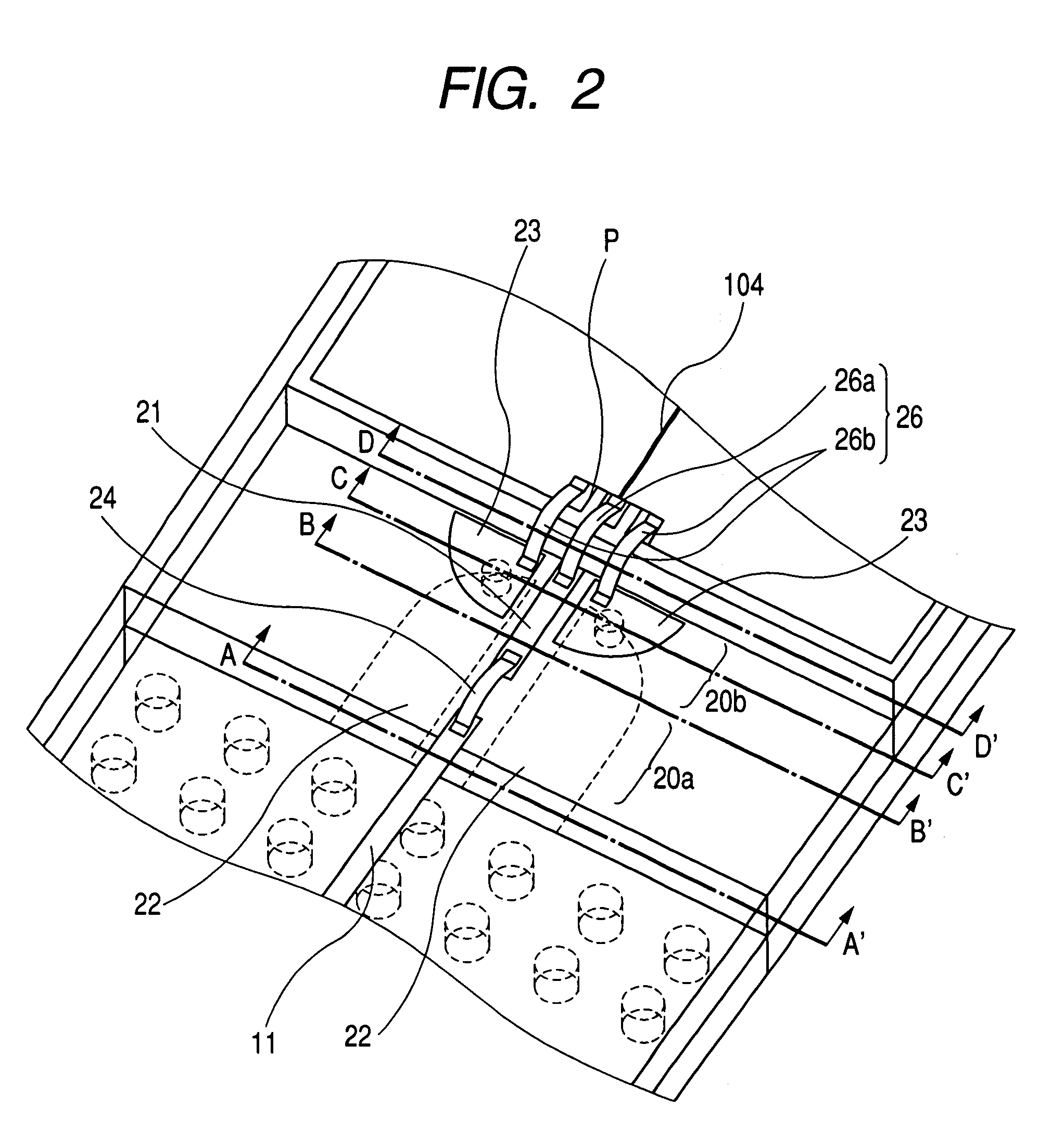
[0041]FIG. 2 is an expanded view of a major portion 1 of the present invention, and FIG. 3A to FIG. 3D shows sections cut along A-A′, B-B′, C-C′ and D-D′, respectively. In FIG. 3A to FIG. 3D, arrows show a direction of the electric field when signals are transmitted. The configuration of the circuit board according to the present invention will be described in more details referring to FIG. 2 and...

second embodiment

[0053]FIG. 7 is a view of a high frequency circuit board according to the Second Embodiment seen from diagonally above. The high frequency circuit board includes a microstrip line 300 and a coplanar line 400 that have the same configurations as the First Embodiment, and ports 1 to 4, and is symmetrically configured laterally and vertically. The high frequency circuit board is also mounted with a chip 200. The chip 200 is formed with two microstrip lines which are configured to connect the port 1 to the port 2, and the port 3 to the port 4, respectively. The chip 200 has the same configuration as the chip 100 except that there are two microstrip lines.

[0054]FIG. 8 shows a result obtained by a simulation on transmission characteristic in the case where the frequency of a signal inputted through the port 1 of the high frequency circuit board according to the Second Embodiment is changed.

[0055]These characteristics are: the transmission characteristic S21 from the port 1 to the port 2, ...


PUM


Abstract

A microstrip line includes a signal strip conductor and a ground conductor. A coplanar line includes two regions. A first region includes a signal strip conductor which is connected to the signal strip conductor of the microstrip line via a wire or the like and a ground strip conductor which continues to the ground conductor. A second region is formed with a ground strip conductor formed above the ground strip conductor via a through hole. A transmission mode changes itself in the microstrip line, the first region of the coplanar line, and the second region of the coplanar line in the sequence as described. This enables converting the transmission mode efficiently from the microstrip line to the coplanar line.

Description

CROSS-REFERENCE TO RELATED APPLICATION[0001]This application is based on and claims the benefit of priority from the earlier Japanese Patent Application NO. 2006-264806 filed Sep. 28, 2006 the description of which is incorporated herein by reference.BACKGROUND OF THE INVENTION[0002]1. Field of the Invention[0003]The present invention relates to a high frequency circuit board which includes a microstrip line and a coplanar line. Further, the present invention relates to a high frequency circuit board which enables transmission of signals with little loss and reflection to semiconductor device by carrying out conversion of a transmission mode from the microstrip line to the coplanar line efficiently and with low loss.[0004]2. Description of the Related Art[0005]Conventionally, a high frequency circuit board using a conversion of a transmission mode from a microstrip line to a coplanar line as disclosed in Japanese Patent Laid-open Publication No. S64-5102, No. 2001-94012, and No. 2001...

Claims


Application Information

Patent Timeline
Patent Type & Authority Patents(United States)
IPC IPC(8): H01P1/16H01P1/00
CPCH01P5/08H01L2224/49175H01L2224/45144H01L2924/00H01L2924/3011H01L2924/30111
Inventor KATAYAMA, TETSUYAUDA, HISANORI
Owner DENSO CORP
Why Eureka
Try Eureka