Controlling power supply to memory cells

a technology of memory cells and power supply, applied in the field of data processing, can solve problems such as the inability to consistently write data values to the cell, and achieve the effect of efficient and effective wri

Active Publication Date: 2010-03-30
ARM LTD
View PDF4 Cites 12 Cited by
  • Summary
  • Abstract
  • Description
  • Claims
  • Application Information

AI Technical Summary

Benefits of technology

[0010]The present invention recognises that the problems that arise due to memory bit cells decreasing in size cannot all be addressed by simply varying the voltage level input to power the cell during a write. It recognises that individual control of the power supplied to the two separate devices forming the bit cell could be used to address the problems of the prior art far more effectively than simply controlling the power source input to both devices. Allowing the power line of each device to be individually controlled provides a cell which can be more readily adjusted such that the problems arising from the different corner cases can be individually addressed and thus, a cell which stores values securely and yet can be consistently written to and read from is provided.
[0014]Although the two power inputs can receive separately controllable either high or low voltage levels, in preferred embodiments it is the high voltage level that is controllable. This is because the arrangement of many traditional memory bit cells means that the control of this high voltage level is the important one for addressing the write problems, in particular it causes a less detrimental reduction in noise margin due to its column based (vertical) control where RNM is affected and not SNM which allows for greater margins. (SNM is signal noise margin when the wordline is open, while RNM: is retention noise margin when the wordline is closed). Controlling the high voltage level differently for each device in a cell enables the cells to be set up to increase performance for both reads and writes and also for the writing of different values. It would be clear to a skilled person that if the memory cells were arranged differently then the control of the low voltage levels may become important.
[0021]The set up of an embodiment of the invention comprises a lay out having an array of cells with two separate high voltage tracks per column and a low voltage track per row. Power control circuitry controls the voltage level supplied to these such that the devices on the cells can receive different high voltage levels. Being able to control the high voltage level differently for each device in a cell enables the performance for both reads and writes to be improved. However, as the control is done per column when the voltage is lowered, it is lowered to the same device in all cells thus, all non-accessed cells are weakened. However, as the write performance for the cell that is accessed is increased the write takes less time and thus, the weakening of the cell by the reduction in the voltage of one of the high power rails occurs for less time than would be the case for a traditional write assist signal.
[0025]The ability to provide separate power control to the two devices can be used to power up the two devices at slightly different times following power up or reset. This enables the memory cells to be initialised in a known state which can in some circumstances be very advantageous. This is particularly so for low power applications, where a memory can be initialised in a known state at power up and the millions of write cycles normally required to achieve this state can be avoided.
[0029]Further control of the power supply to the two devices not only in response to the type of data access request but also to the data that is being written means that the devices can individually be held at appropriate levels for the data that they are to receive not only enabling data to be consistently successfully written to the cells but also increasing the performance of such a write.
[0031]When a data 0 is to be written then the two devices store opposite values to those that they stored for the 1. Thus, controlling the power supply to the devices in the opposite manner to that which was done for write of the data 1 produces an efficient and effective write.

Problems solved by technology

The traditional six transistor bit cell is widely used for storing data and suffers from the problem of being unable to consistently write data values to the cell in circumstances where the cells are reduced in size and where the smaller process technology nodes suffer from yield limiting process variations.

Method used


Image

  • Controlling power supply to memory cells
  • Controlling power supply to memory cells
  • Controlling power supply to memory cells

Examples


Embodiment Construction

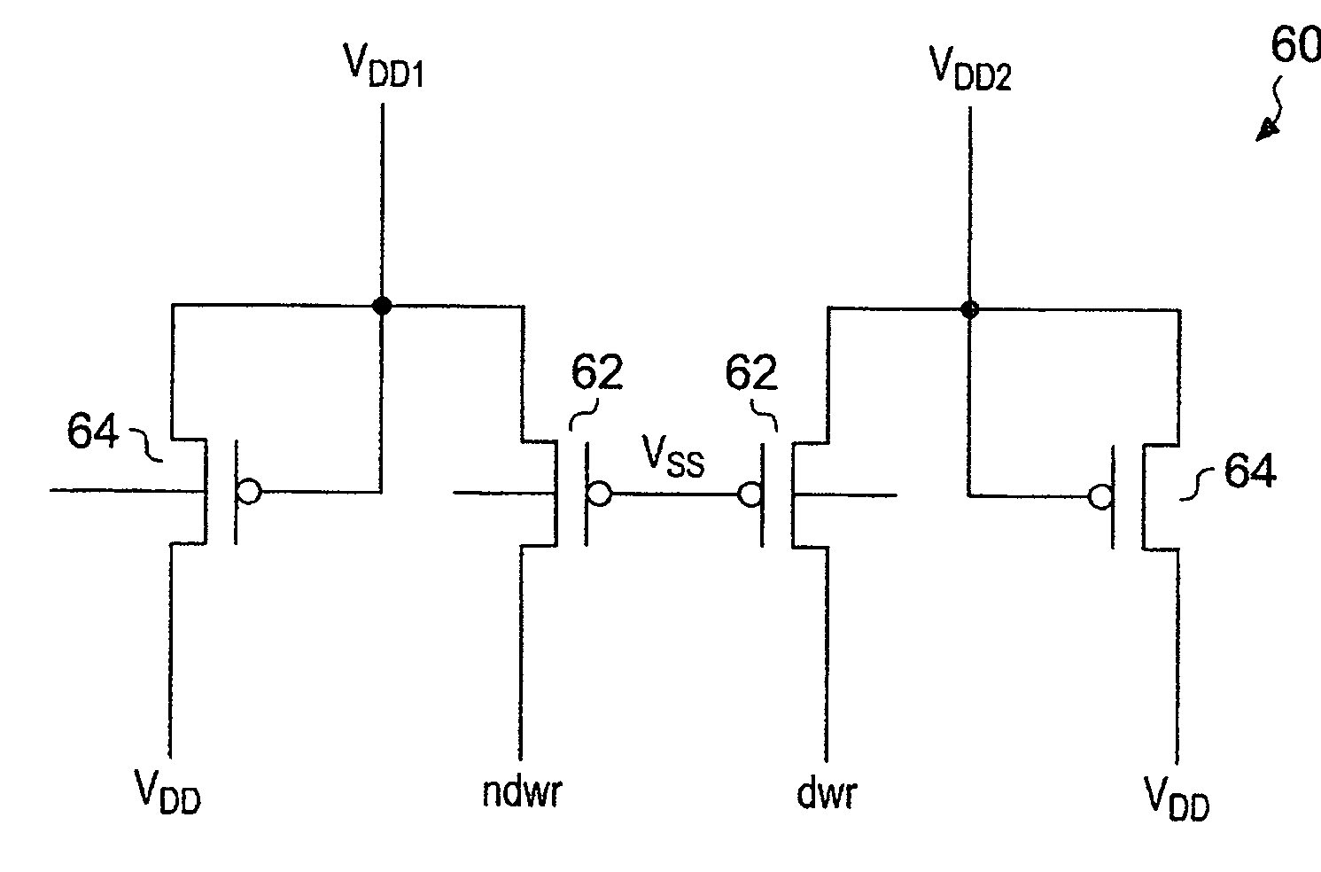
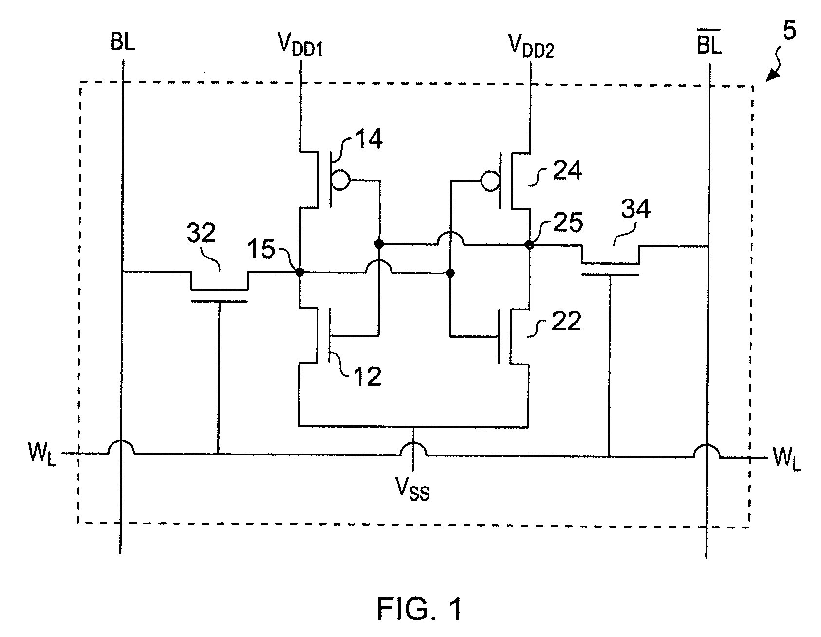
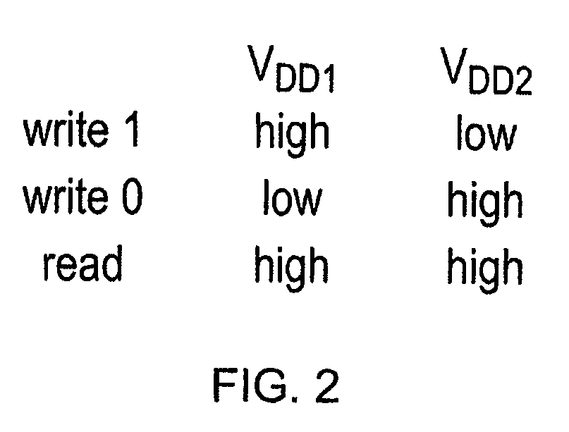
[0046]FIG. 1 illustrates a memory cell 5 according to an embodiment of the present invention. The memory cell 5 comprises a pair of cross-coupled inverters formed by transistors 12, 14, 22 and 24. Transistors 12 and 14 form a first device which is powered by VDD 1 while transistors 22 and 24 form a second device powered by VDD 2. These two devices have a common low voltage rail VSS.

[0047]The memory cell further comprises bit lines BL and a word line WL. The word line is connected to the gates of two access transistors 32 and 34 which when switched on by a signal on this word line provide a path between an input / output portion 15, 25 of the devices and the bit lines. Thus, under control of the word line the devices can be placed in data communication with the bit lines and data can be read in or written out from these devices.

[0048]As the two devices are a cross coupled pair if device 1, transistors 12 and 14 has a 1 at input / output port 15 then second device transistors 22, 24 will ...


PUM


Abstract

A semiconductor memory storage cell and a memory comprising an array of these storage cells is disclosed. The storage cell comprising: a feedback loop comprising two devices for storing opposite binary values; data input and output for inputting data to and outputting data from said two devices; and each of said two devices comprising a power source input, such that each device can be powered independently of the other.

Description

BACKGROUND OF THE INVENTION[0001]1. Field of the Invention[0002]The field of the invention relates to data processing and in particular to memory storage cells.[0003]2. Description of the Prior Art[0004]Memory storage cells formed from semiconductors in integrated circuits are known. They are conventionally formed of bistable circuits that can be flipped between one of two stable states. If the circuits are well balanced then they do not preferentially store either state. A well balanced cell that does not preferentially store a particular value will have the advantage of holding either value with approximately the same power loss and will be as easy to write a “one” to as it is to write a “zero”. However, a potential drawback of such a cell is that on power up it is unknown which value will to be stored in these cells and there are circumstances where it would be advantageous to initialise a memory in a known state.[0005]There is a continual demand to reduce the size and power cons...

Claims


Application Information

Patent Timeline
Patent Type & Authority Patents(United States)
IPC IPC(8): G11C7/00
CPCG11C5/14
Inventor HOLD, BETINA
Owner ARM LTD
Why Eureka
Try Eureka