

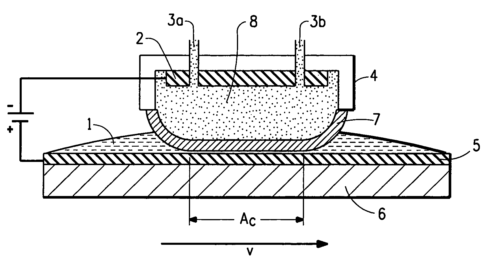
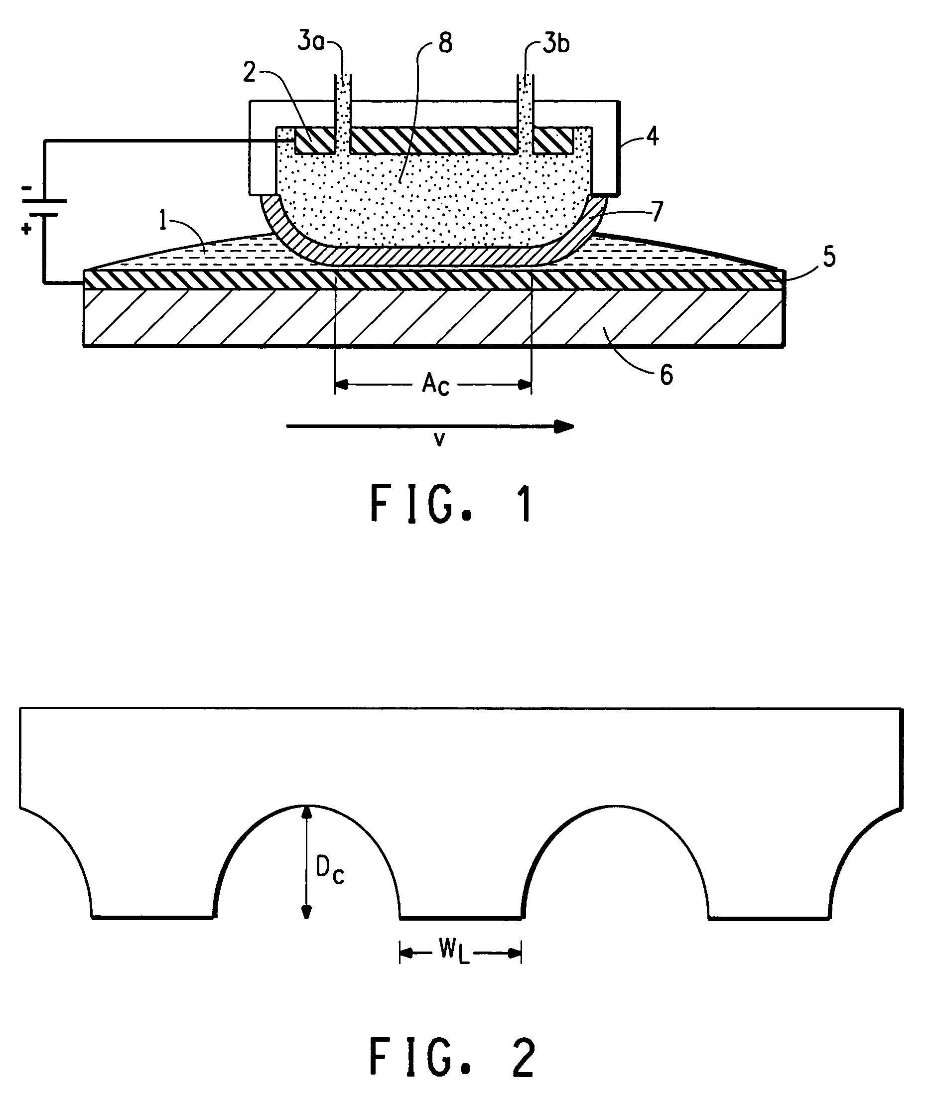
Membrane-mediated electropolishing with topographically patterned membranes
a membrane-mediated electropolishing and topographic pattern technology, applied in the direction of machining electrodes, electrical-based machining electrodes, manufacturing tools, etc., can solve the problems of incompatible mechanically fragile materials, high cost of cmp, and waste of resources
- Summary
- Abstract
- Description
- Claims
- Application Information
AI Technical Summary
Benefits of technology
Problems solved by technology
Method used
Image

Examples
example 1
Preparation of a Topographically Patterned Membrane
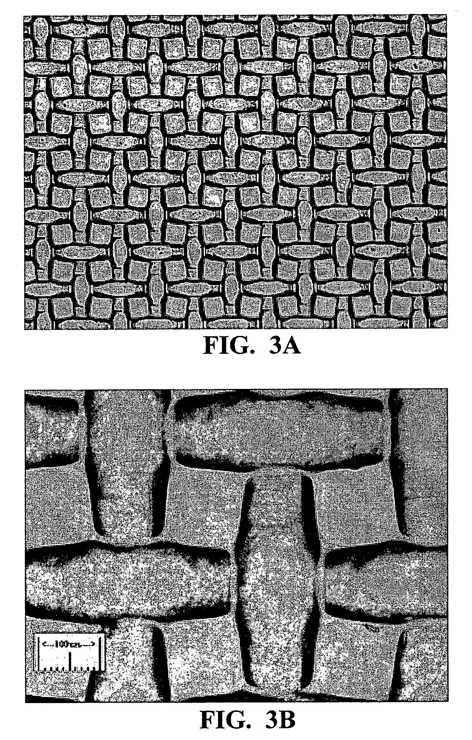
[0093]A topographically patterned membrane was prepared by embossing a smooth flat Nafion® N117 membrane (0.007″ thick) using as the embossing tool a wire mesh comprising 0.0045″ stainless steel wires woven at 100×100 wires / inch. The wire mesh was first flattened in a hydraulic press at 30,000 psi in order to minimize thickness variations where the wires crossed. The flattened mesh was pressed between two samples of N117 film at approximately 80° C. and 1000 psi, then cooled to ambient temperature before releasing the pressure and separating the films. FIGS. 3A and 3B show optical micrographs of the embossed membrane. The square areas in these micrographs are the projecting lands while the recessed channels are seen as casts of the crossing pattern of wires. FIGS. 4A and 4B show micrographs of the static etch pattern on a Cu work-piece created by the same membrane from which the interfacial area of each land (1.4×10⁻⁴ cm2) and fract...
example 2
Comparative Performance of Smooth and Embossed Membranes
[0094]Data comparing the performance of smooth and topographically patterned membranes are summarized in FIGS. 6-11.
[0095]FIGS. 6 and 7 show polarization curves (variations in the steady-state current density with voltage) respectively for smooth and embossed membranes at constant Ph and a range of interface velocities. For applied voltages greater than 2V, the interfacial current density Ii for the embossed membrane is substantially higher than for the smooth membrane and that interface velocity has a strong influence on the smooth membrane but very little on the embossed membrane.
[0096]FIGS. 8 and 9 show polarization curves respectively for smooth and embossed membranes at constant v and different values of Ph. The embossed membrane provides much higher current density at for applied voltages greater than 2V, and much less sensitivity to Ph.
[0097]FIG. 10 shows variations in the net current density i with interface velocity v ...
example 3
Planarization Efficiency with an Embossed Membrane at High Removal Rate
[0099]FIG. 12 shows the results of planarizing a Cu damascene test wafer by MMEP using an embossed Nafion® membrane with land areas 2.8×10⁻⁴ cm2 and fractional coverage FL 0.24. The voltage was pulsed between 0.1 msec at 1V and 0.2 msec at 8 V. The average current density was Ic˜1 amp / cm2 and n˜5 corresponding to an interfacial removal rate within the contour area RRc˜6 μm / min. Therefore to achieve RR>1 μm / min over the entire work-piece would require a contour area or plurality of contour areas no greater than 17% of the total area of the work-piece. In FIG. 12 the step height at 100 μm lines and spaces is plotted as a function of the average amount of Cu removed, as determined from sheet resistance measurements and weight loss. The data points represent measurements at 6 different radial positions (designated R) across the surface of the 200 mm wafer. The data show that planarization was highly uniform and compl...
PUM
| Property | Measurement | Unit |
|---|---|---|
| pKa | aaaaa | aaaaa |
| conductivity | aaaaa | aaaaa |
| conductivity | aaaaa | aaaaa |
Abstract
Description
Claims
Application Information