Semiconductor memory device including pillar-shaped semiconductor layers and a method of fabricating the same

a semiconductor and memory device technology, applied in semiconductor devices, electrical appliances, instruments, etc., can solve the problems of injuring process reliability, limiting miniaturization, and increasing the memory density based on multi-level storage schemes also has a limit defined by data reliability,

Inactive Publication Date: 2010-04-13
KK TOSHIBA
View PDF11 Cites 212 Cited by
  • Summary
  • Abstract
  • Description
  • Claims
  • Application Information

AI Technical Summary

Problems solved by technology

However, there is a limit for miniaturization.
The increase of memory density based on the multi-level storage scheme also has a limit defined by data reliability.
However, there are some problems in the disclosed method in this document as follows.
It will not only injure the process reliability but also cause the memory cell's operation delay.
Therefore, the number of processes is increased in proportion to the number of memory cells, and it leads to reliability reduction.
There is not provided a measure for avoiding such the problem.
If as it is, it is impossible to achieve a desired operation of a NAND-type flash memory
Therefore, there is a limit for making the resistance of the word lines and select gate lines low, and it is difficult to achieve a usual NAND-type flash memory.

Method used


Image

  • Semiconductor memory device including pillar-shaped semiconductor layers and a method of fabricating the same
  • Semiconductor memory device including pillar-shaped semiconductor layers and a method of fabricating the same
  • Semiconductor memory device including pillar-shaped semiconductor layers and a method of fabricating the same

Examples


embodiment 1

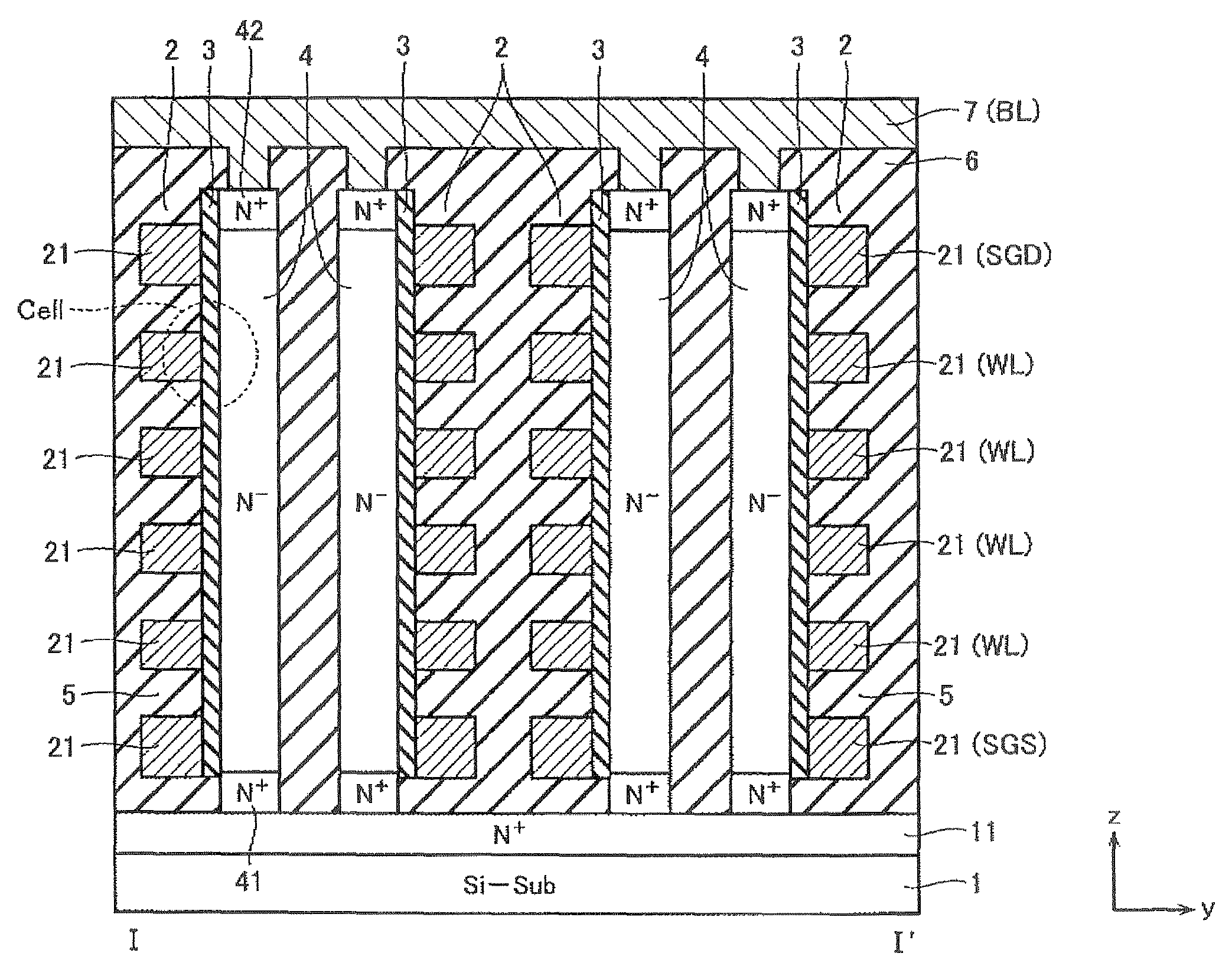
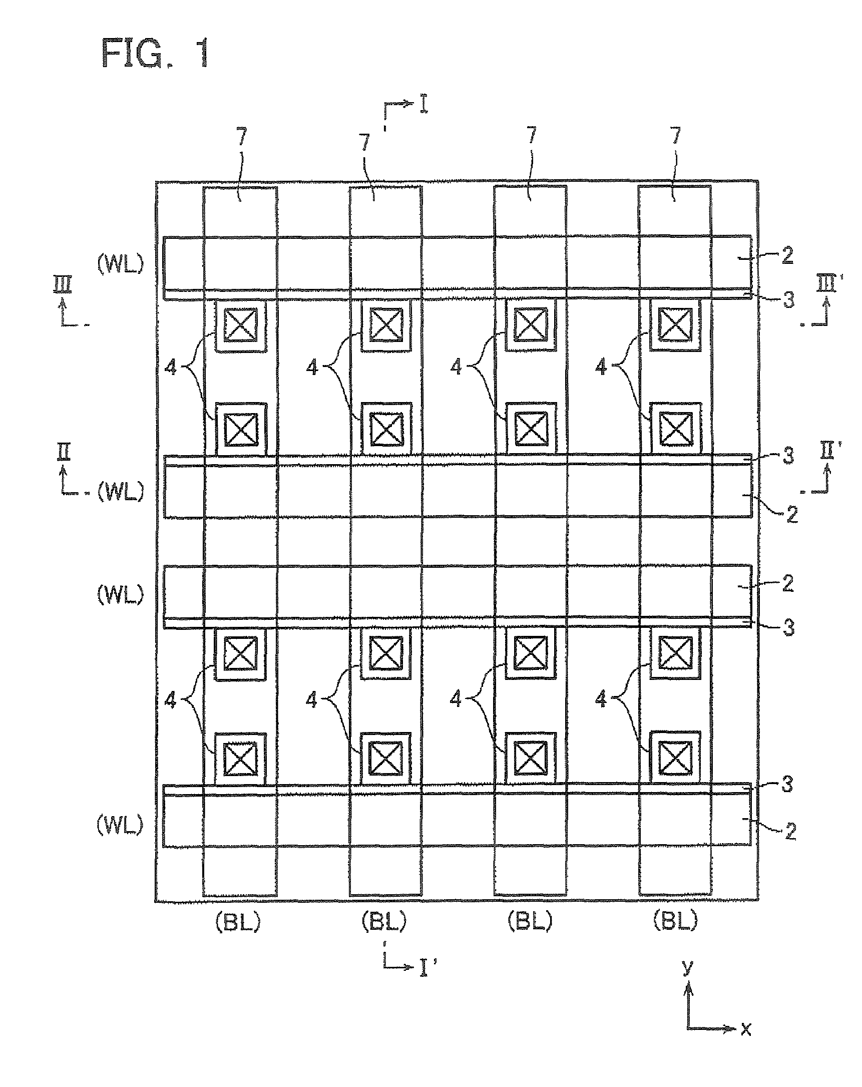
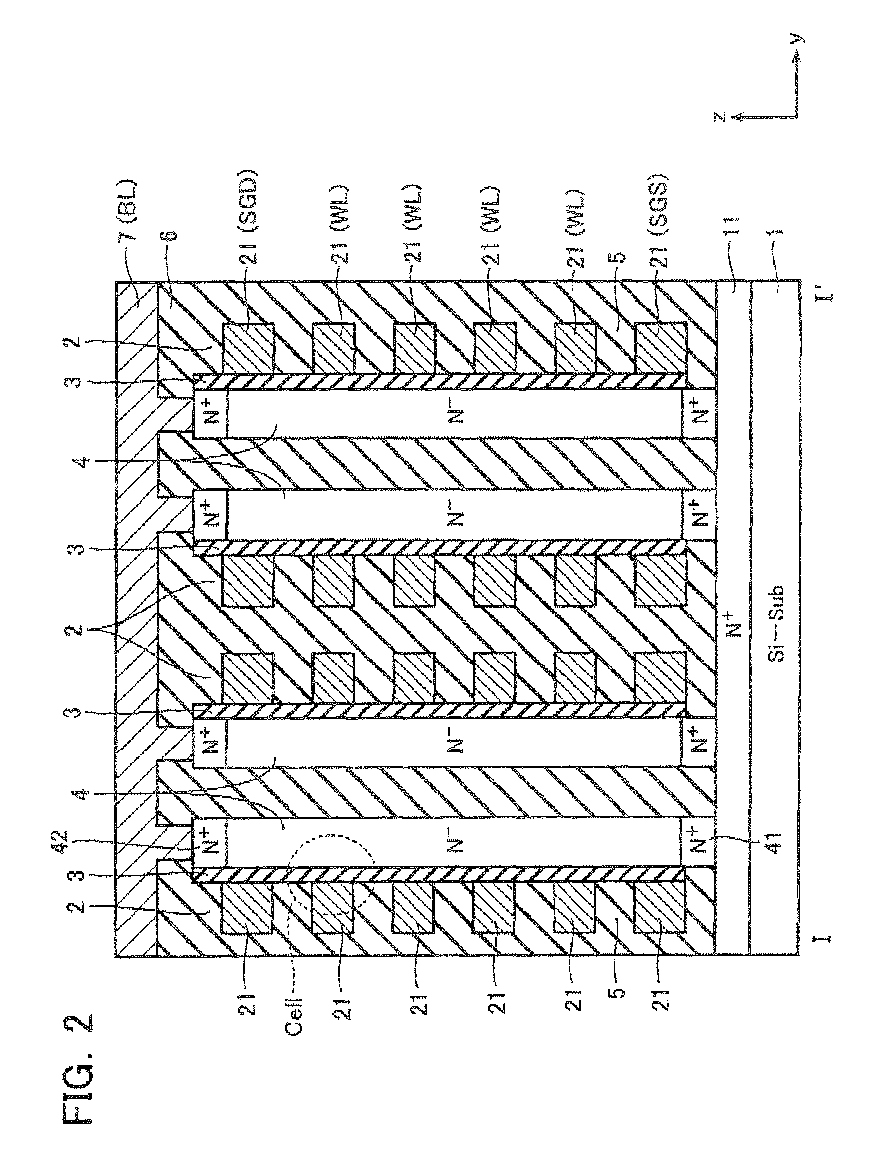
[0097]FIG. 1 is a plan view of a memory cell array of a NAND-type flash memory In accordance with an embodiment, and FIGS. 2, 3 and 4 are sectional views thereof taken along lines I-I′, II-II′ and III-III′ in FIG. 1, respectively.

[0098]A plurality of gate wiring stack bodies 2 are formed on a silicon substrate 1, each of which has multiple gate wirings 21 stacked and separated from each other with interlayer dielectric films 5 interposed therebetween. Each of the gate wiring stack bodies 2 is patterned as elongated in x-direction in the x-y plane of the substrate 1.

[0099]The gate wirings 21 are formed of a metal film, the resistance of which is lower than that of a polycrystalline silicon film, for example, selected from tungsten (W) aluminum (Al), cupper (Cu), silicide thereof and the like. Alternatively, the gate wirings 21 may be initially formed as polycrystalline silicon wirings, and then reformed as silicide wirings by a salicide (Self Aligned Silicide) step. As a result, it i...

embodiment 2

[0147]FIGS. 23 and 24 are a plan view and I-I′ sectional view thereof, respectively, of a memory cell array in a NAND-type flash memory in accordance with Embodiment 2, which correspond to FIGS. 1 and 2, respectively.

[0148]In Embodiment 1, pillar-shaped silicon layers 4 are disposed in relation with the gate wiring stack bodies 2 in such a manner that one array is opposite to one side surface of a gate wiring stack body; and the following one to the reverse side surface of the following gate wiring stack body. By contrast, in this embodiment, pillar-type silicon layers 4 are disposed opposite to the same side surfaces of the respective gate wiring stack bodies 2.

[0149]Others are the same as in Embodiment 1. That is, one side surface of the pillar-shaped silicon layer 4 is opposite to the gate wiring stack body 2 while the remaining three side surfaces are in contact with device isolating film; II-II′ and is III-III′ sectional views of FIG. 23 are identical with those shown in FIGS. ...

embodiment 3

[0150]FIG. 25 is a plan view of a memory cell array in a NAND-type flash memory in accordance with Embodiment 3, which corresponds to FIG, 1 in Embodiment 1. FIG. 26 is I-I′ sectional view of FIG. 25 II-II′ and III-III′ sectional views of FIG. 25 are identical with those shown in FIGS. 3 and 4; and fabrication processes are the same as in Embodiment 1.

[0151]In Embodiment 1, two arrays of pillar-shaped silicon layers 4 are disposed between two gate wiring stack bodies 2 to be driven with them. By contrast, in this Embodiment 3, adjacent two gate wiring stack bodies share one array of pillar-shaped silicon layers 4. In other words, in Embodiments 1 and 2, one side surface of each pillar-shaped silicon layer 4 is opposite to the gate wiring stack body 2 and the remaining three side surfaces are in contact with the device isolating film, while in this Embodiment 3, opposite side surfaces of the pillar-shaped silicon layer 4 are opposite to adjacent two gate wiring stack bodies 2, respec...


PUM


Abstract

A semiconductor memory device includes: a semiconductor substrate, on which an impurity diffusion layer is formed in a cell array area; a gate wiring stack body formed on the cell array area, in which multiple gate wirings are stacked and separated from each other with insulating films; a gate insulating film formed on the side surface of the gate wiring stack body, in which an insulating charge storage layer is contained, pillar-shaped semiconductor layers arranged along the gate wiring stack body, one side surfaces of which are opposed to the gate wiring stack body via the gate insulating film, each pillar-shaped semiconductor layer having the same conductivity type as the impurity diffusion layer; and data lines formed to be in contact with the upper surfaces of the pillar-shaped semiconductor layers and intersect the gate wirings.

Description

CROSS-REFERENCE TO RELATED APPLICATION[0001]This application is based on and claims the benefit of priority from the prior Japanese Patent Application No. 2005-379017, filed on Dec. 28, 2005, the entire contents of[0002]which are incorporated herein by referenceBACKGROUND OF THE INVENTION[0003]1. Field of the Invention[0004]This invention relates to an electrically rewritable and non-volatile semiconductor memory device (EEPROM), more particularly relates to such a device that multiple memory cells are stacked on a semiconductor substrate to constitute a NAND cell unit, and a method of fabricating the same.[0005]2. Description of the Related Art[0006]A NAND-type flash memory is known as one of EEPROMs. In the NAND-type flash memory, multiple memory cells are connected in series in such a manner that adjacent two cells share a source / drain diffusion layer, thereby constituting a NAND cell unit. By use of this cell array arrangement, the unit cell area is smaller that that of a NOR-ty...

Claims


Application Information

Patent Timeline
Patent Type & Authority Patents(United States)
IPC IPC(8): H01L27/115
CPCH01L27/105H01L27/115H01L27/11551H01L27/11556H01L29/7926H01L27/11578H01L27/11582H01L29/4234H01L29/66833H01L29/792H01L27/11568G11C16/0483H10B69/00H10B41/20H10B41/27H10B43/30H10B43/20H10B43/27
Inventor ARAI, FUMITAKASHIROTA, RIICHIROMIZUKAMI, MAKOTO
Owner KK TOSHIBA
Why Eureka
Try Eureka