On-chip decoupling capacitance and power/ground network wire co-optimization to reduce dynamic noise

a technology of power/ground network wire and capacitance decoupling, which is applied in the field of on-chip decoupling capacitance and power/ground network wire cooptimization to reduce dynamic noise, and can solve the problems of chip design, ever increasing removal, and chip circuit malfunction

Inactive Publication Date: 2010-04-13
NXP USA INC
View PDF7 Cites 20 Cited by
  • Summary
  • Abstract
  • Description
  • Claims
  • Application Information

AI Technical Summary

Problems solved by technology

As the design and layout of semiconductor circuits, or microcircuits, or chips, become more complex, and in particular, as there is an increase in complexity of very large scale integration (VLSI) layout, an increase in operational frequency and the use of supply voltage scaling, there is an ever increasing need to remove or reduce undesired noise from the chip design.
A chip's power distribution network is a major noise source as the fluctuations in supply voltage due to the parasitic resistance, inductance and capacitance in the network alter signals' voltage levels and can cause malfunctioning of the chip's circuits.
Designing a robust power distribution network for low dynamic voltage fluctuations has become a challenging task.
Extremely dense and complex circuit layouts for high frequency operation necessitate reduction of these undesired noise levels, especially at some sensitive parts of circuits such as clock generators and analog circuits.
Sometimes circuit density does not allow sufficient white space to effectively add decaps near a hot spot region.
This diminishes the effectiveness of the decap and requires more decap to be added.
However, the decoupling capacitance density achievable may be limited by the process technology and by the limited amount of white space available around a problem spot.
Because of this, it is not always possible to place the entire amount of required decap close enough to a hot spot region to achieve effective dynamic noise reduction.
As understood in the art, decap budgeting and placement is a non-linear optimization problem.
Several known solution methods make very simple calculations for decap, resulting in overestimation.
These methods are not practical for very large chip designs as the computation of adjoint sensitivities, or gradients, and the non-linear optimization are both very expensive in runtime and memory resources.
Further complicating the problem, these techniques add decap and recompute sensitivity in an iterative procedure.
As the complexity of one adjoint sensitivity computation is the same as one transient analysis, the iterative nonlinear optimization procedure becomes quite expensive and time consuming.
In addition, the adjoint sensitivity calculation typically needs to store waveforms at every node in both the original and the adjoint networks, which may exhaust the memory resource for large networks.
An approximate lumped decoupling capacitance is estimated for each floor plan module, with an assumption that the original voltage of decoupling capacitance is a perfect VDD voltage reference; however, the parasitic capacitance and existing decap value are not considered in these methods, which causes inaccuracies.

Method used


Image

  • On-chip decoupling capacitance and power/ground network wire co-optimization to reduce dynamic noise
  • On-chip decoupling capacitance and power/ground network wire co-optimization to reduce dynamic noise
  • On-chip decoupling capacitance and power/ground network wire co-optimization to reduce dynamic noise

Examples


Embodiment Construction

[0021]In the following detailed description of exemplary embodiments of the invention, specific exemplary embodiments in which the invention may be practiced are described in sufficient detail to enable those skilled in the art to practice the invention, and it is to be understood that other embodiments may be utilized and that logical, architectural, programmatic, mechanical, electrical and other changes may be made without departing from the spirit or scope of the invention. The following detailed description is, therefore, not to be taken in a limiting sense, and the scope of the invention is defined only by the appended claims.

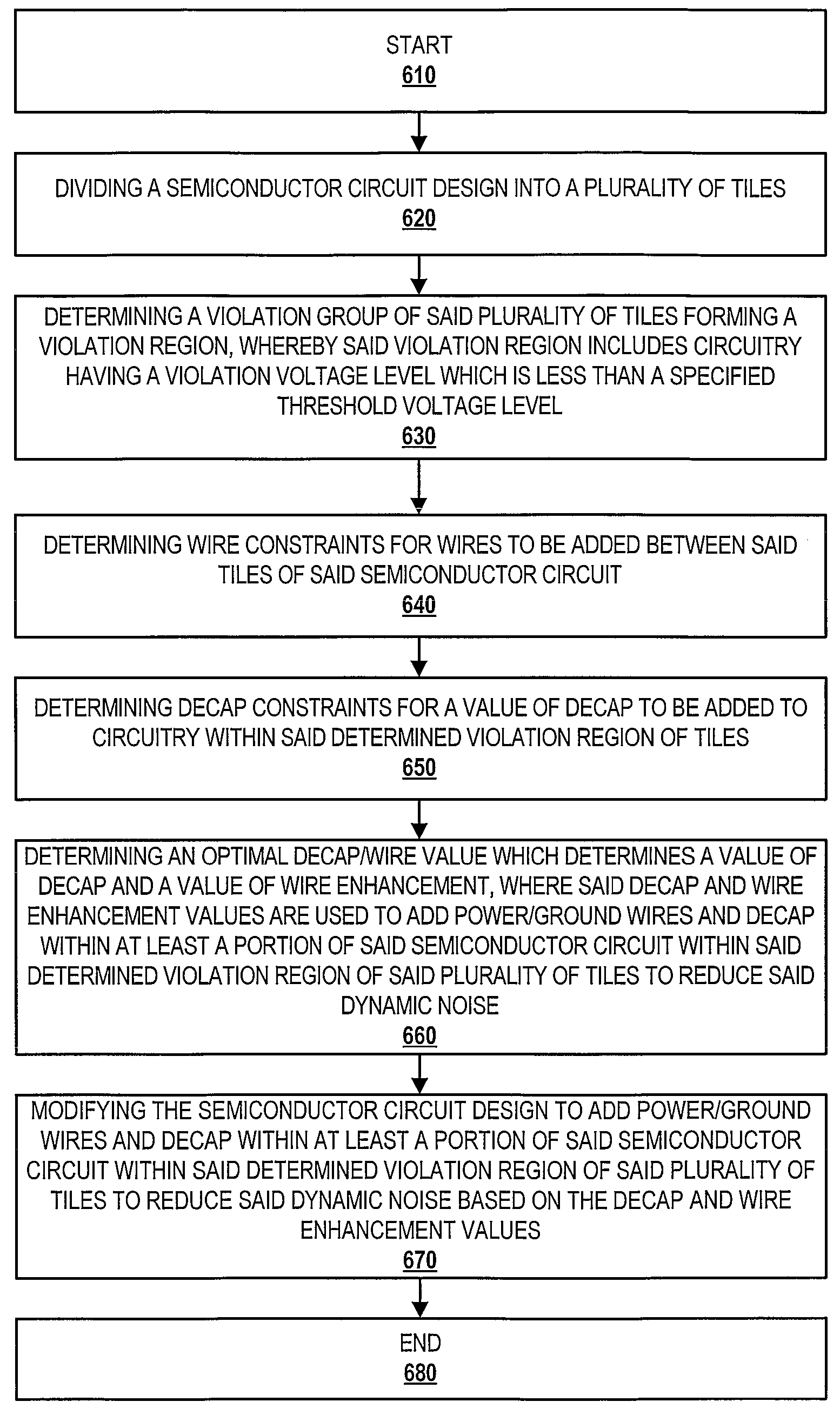
[0022]The method of a preferred embodiment eliminates the problems of the techniques found in the prior art and determines the optimal amount of and the location for decaps, to reduce dynamic supply noise in a circuit quickly and accurately. The method of a preferred embodiment also determines whether local wiring enhancements should be made to further red...


PUM


Abstract

A semiconductor power network (100) decoupling capacitance (decap) budgeting problem is co-optimized with a wiring enhancement problem, wherein the solution is formulated to minimize the total decap to be added or wiring changes (addition of wires (420)) to be made to the network (100). Voltage constraints, available white space and other constraints determine the amount of decap to be added. Wire enhancements and / or added decap can be distributed throughout a violation region (120) of the semiconductor circuit (100) design to reduce dynamic supply voltage noise so that dynamic network voltages are at all times maintained greater than a user-specified threshold voltage level (220).

Description

BACKGROUND OF THE INVENTION[0001]1. Field of the Invention[0002]The invention relates generally to a device and method of determining the amount and location of decoupling capacitance or enhanced local wiring to be added during the design and layout of a semiconductor circuit to optimally reduce dynamic supply voltage fluctuations during circuit operation.[0003]2. Description of the Related Art[0004]As the design and layout of semiconductor circuits, or microcircuits, or chips, become more complex, and in particular, as there is an increase in complexity of very large scale integration (VLSI) layout, an increase in operational frequency and the use of supply voltage scaling, there is an ever increasing need to remove or reduce undesired noise from the chip design. A chip's power distribution network is a major noise source as the fluctuations in supply voltage due to the parasitic resistance, inductance and capacitance in the network alter signals' voltage levels and can cause malfu...

Claims


Application Information

Patent Timeline
Patent Type & Authority Patents(United States)
IPC IPC(8): G06F17/50
CPCG06F17/5077G06F17/5036G06F30/367G06F30/394
Inventor ZHAO, MINPANDA, RAJENDRAN
Owner NXP USA INC
Why Eureka
Try Eureka