Semiconductor manufacturing process monitoring

a technology of semiconductor manufacturing and process monitoring, applied in the field of process control, can solve problems such as the challenge of monitoring a semiconductor manufacturing lin

Inactive Publication Date: 2010-05-18
GLOBALFOUNDRIES INC
View PDF9 Cites 409 Cited by
  • Summary
  • Abstract
  • Description
  • Claims
  • Application Information

AI Technical Summary

Problems solved by technology

With many process tools, each having possibly hundreds of individual parameters, the task of monitoring a semiconductor manufacturing line can be challenging.

Method used


Image

  • Semiconductor manufacturing process monitoring
  • Semiconductor manufacturing process monitoring
  • Semiconductor manufacturing process monitoring

Examples


Embodiment Construction

[0046]Reference will now be made in detail to the presently preferred embodiments of the invention, examples of which are illustrated in the accompanying drawings.

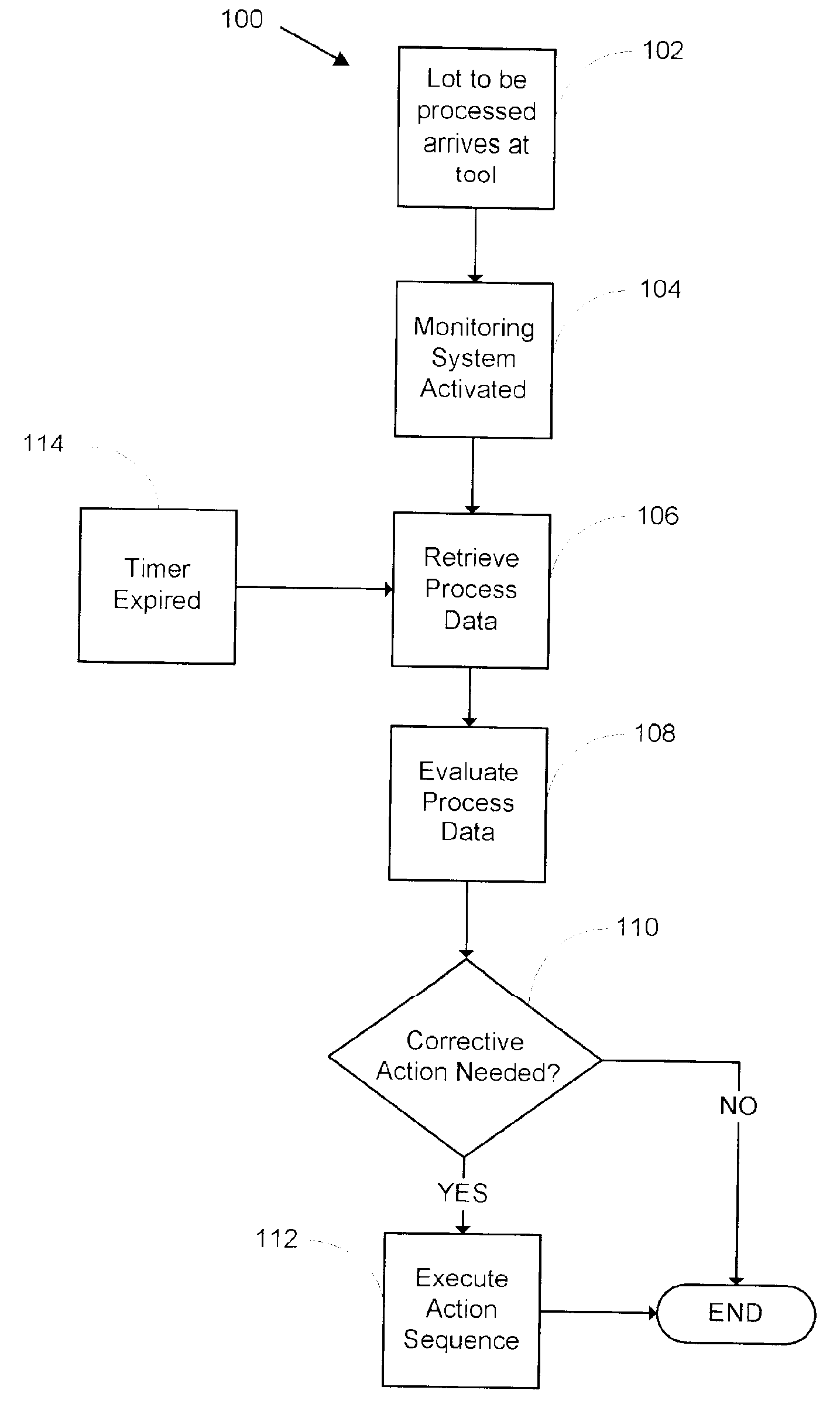
[0047]FIG. 1 is a flowchart 100 indicating process steps for carrying out the method of the present invention. In step 102, the lot of wafers arrives at a process tool. The process tools monitored by the present invention may include, but are not limited to, the following process tool types:[0048]Chemical Vapor Deposition Tool (CVD)[0049]Physical Vapor Deposition Tool (PVD)[0050]Stepper Tool[0051]Sputter Tool[0052]Spinner Tool[0053]Tube Furnace[0054]Reactive Ion Etch Tool (RIE)[0055]Aligner[0056]Ion Implantation System[0057]Electrochemical Plating Tool (ECP)[0058]Chemical Mechanical Polish Tool (CMP)

[0059]Typically the lot of wafers to be processed will arrive at a process tool via a wafer carrier. The wafer carrier is preferably handled by the AMHS to transport the lot to the various process tools needed to complete the m...


PUM


Abstract

A system and method for monitoring a semiconductor manufacturing process is disclosed. The system communicates with one or more process tools, and monitors each tool during a predetermined process window time. Errors and warnings are provided to users, allowing corrective action to be taken. Additionally, the system of the present invention can initiate automatic adjustment of the process tools to maintain an efficient manufacturing operation.

Description

FIELD OF THE INVENTION[0001]This invention is generally related to semiconductor fabrication. More specifically, this invention relates to process control in a semiconductor manufacturing environment.BACKGROUND[0002]Integrated circuits are typically formed by processing several semiconductor wafers as a group or “lot” through a series of wafer fabrication process tools (hereafter, “process tools”). Each process tool typically performs a single wafer fabrication operation upon the semiconductor wafers. The integrated circuits formed in this manner are substantially identical to one another. Following wafer fabrication, the integrated circuits are typically subjected to functional testing, and then separated to form individual integrated circuits called “chips” or “die.” Fully functional die are typically packaged and sold as individual units.[0003]During operation of a process tool, one or more operating conditions are established within the process tool, typically dependent upon inp...

Claims


Application Information

Patent Timeline
Patent Type & Authority Patents(United States)
IPC IPC(8): G06F19/00G05B23/02G05B9/02G21C17/00G06F11/30
CPCG05B19/4184G05B19/41875G05B2219/31355G05B2219/31356G05B2219/45031G05B2219/32179G05B2219/32182G05B2219/32209G05B2219/31365Y02P90/02
Inventor MENSER, JR., CLAYTON DAVIDGILFFORD, JEFFREY PAUL
Owner GLOBALFOUNDRIES INC
Why Eureka
Try Eureka