
CMOS image sensor and method for fabricating the same

a technology of image sensor and manufacturing method, which is applied in the direction of diodes, radiation control devices, semiconductor devices, etc., can solve the problems of complex fabrication process requiring multi-phase photo process, high power consumption, and complicated driving method, and achieve the effect of enhancing the light-receiving capability of image sensors

Inactive Publication Date: 2010-05-25
DONGBU ELECTRONICS CO LTD
View PDF13 Cites 10 Cited by
  • Summary
  • Abstract
  • Description
  • Claims
  • Application Information

AI Technical Summary

Benefits of technology

"The present invention is a CMOS image sensor and a method for fabricating it that enhances the light-receiving capability of an image sensor by configuring a microlens to comprise central and peripheral parts. Each of the central and peripheral parts are imparted with a predetermined convex curvature to maximize light transmitted to an active device for generating an electrical charge according to the intensity of an incoming light signal. The CMOS image sensor has at least one microlens formed by anisotropic etching to have a focusing centerline, a central lens portion, and a peripheral lens portion. The method of fabricating the CMOS image sensor includes forming at least one photodiode, a color filter layer, a planarizing layer, a first insulating layer to have a microlens pattern, a second insulating layer to have a sidewall pattern, and at least one microlens by an anisotropic etching of the microlens pattern and the sidewall pattern. The technical effects of the invention are improved light-receiving capability, higher sensitivity, and better image quality."

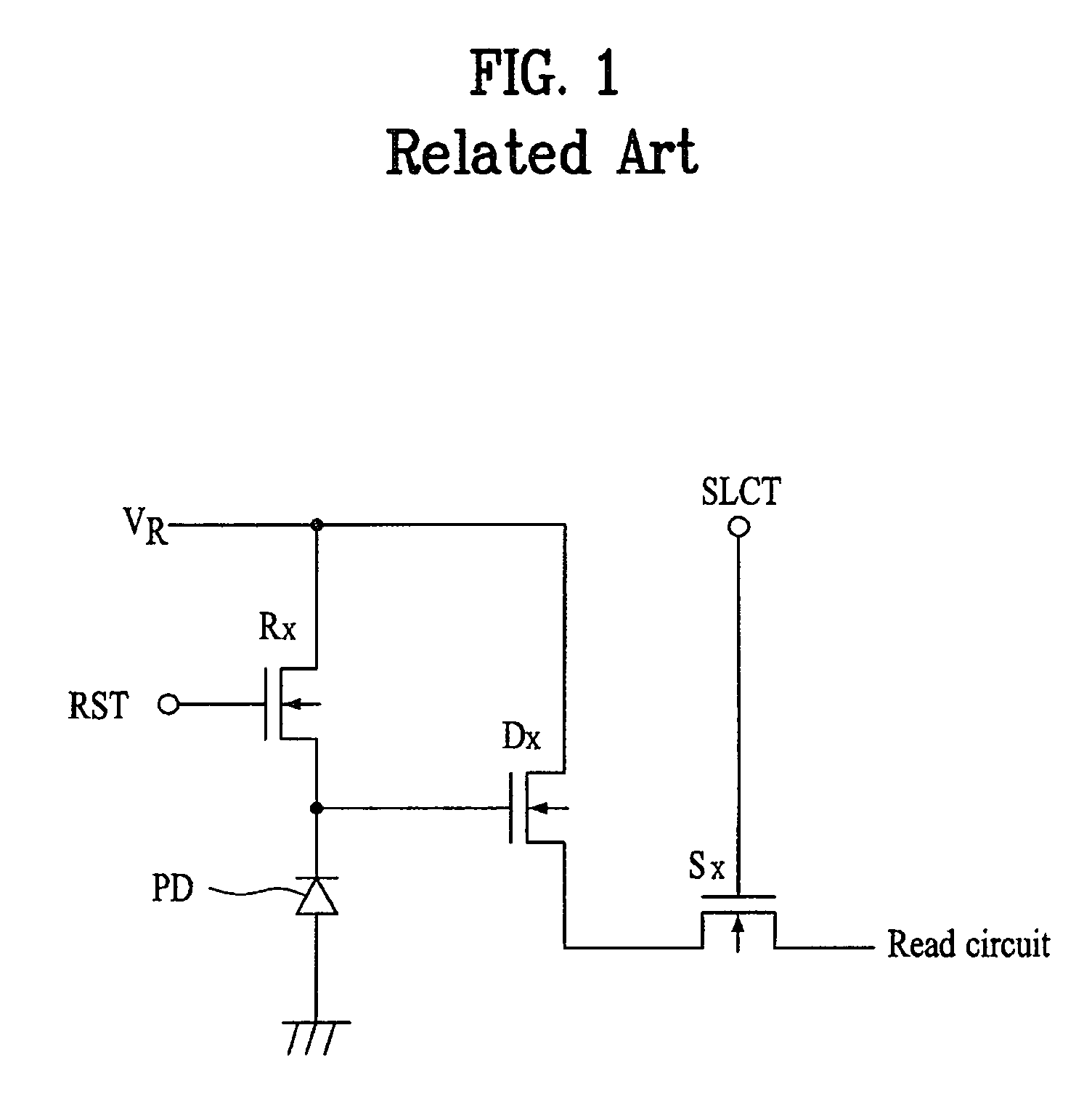
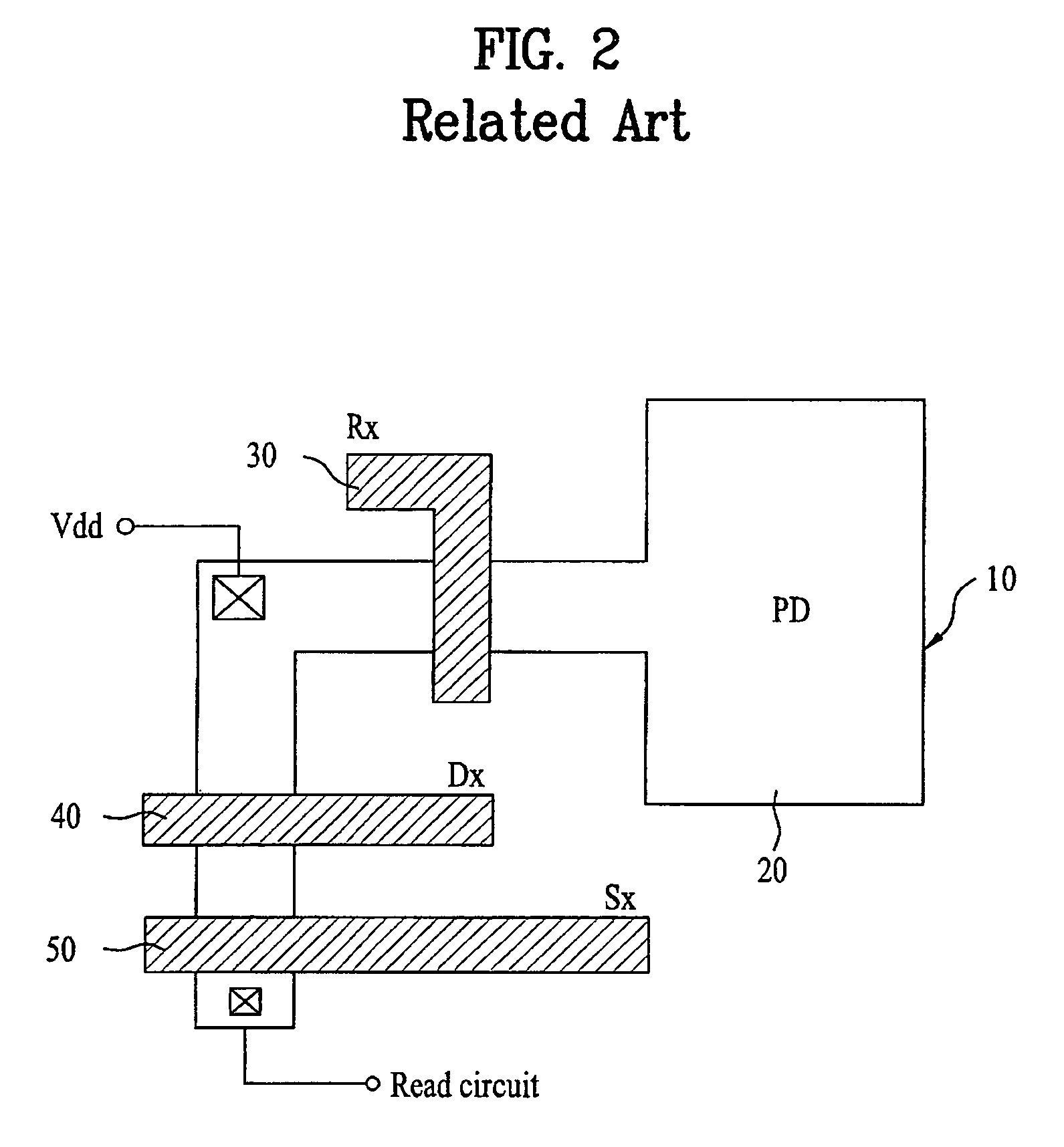
Problems solved by technology

Disadvantages of a general charge-coupled device include a complicated driving method, high power consumption, and a complicated fabrication process requiring a multi-phased photo process.
In a charge-coupled device, integration of complementary circuitry such as a control circuit, a signal processor, and an analog-to-digital converter into a single-chip device is difficult.
Thus, development of compact-sized or thin products is hindered.
However, there is a limit to increasing the photo-sensing portion due to the required presence of the logic circuit portion.

Method used


Image

  • CMOS image sensor and method for fabricating the same
  • CMOS image sensor and method for fabricating the same
  • CMOS image sensor and method for fabricating the same

Examples


Embodiment Construction

[0028]Reference will now be made in detail to embodiments of the present invention, examples of which are illustrated in the accompanying drawings. Wherever possible, like reference designations will be used throughout the drawings to refer to the same or similar parts.

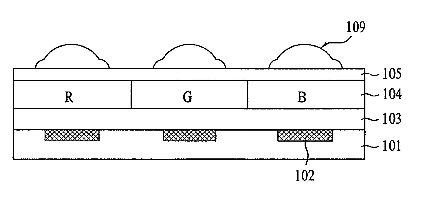
[0029]Referring to FIG. 6A, an insulating interlayer 103 is formed on a semiconductor substrate 101 having at least one photodiode 102 formed in a predetermined surface of the semiconductor substrate. Each photodiode is configured with various transistors (not shown) and a unit pixel of the CMOS image sensor is formed. Photodiodes 102 are active devices for generating an electrical charge according to the intensity of an incoming light signal and may be a photo-gate type device. The insulating interlayer 103 may include an optical shielding layer (not shown) to prevent light from entering a substrate area other than at one of the photodiodes 102. A color filter layer 104, comprised of an array of red (R), green (G), a...


PUM


Abstract

A CMOS image sensor and fabricating method thereof enhances a light-receiving capability of an image sensor by preventing poor light-refraction characteristics at the peripheral part of a microlens. The CMOS image sensor includes at least one microlens formed by anistropic etching to have a focusing centerline, a central lens portion, and a peripheral lens portion, wherein the focusing centerline passes through the central lens portion and wherein the peripheral lens portion surrounds the central lens portion. The central lens portion has a first convex curvature based on a first radius and the peripheral lens portion has second convex curvature based on a second radius, wherein the second radius is greater than the first radius.

Description

[0001]This application claims the benefit of Korean Patent Application No. 10-2004-0090796, filed on Nov. 9, 2004, which is hereby incorporated by reference for all purposes as if fully set forth herein.BACKGROUND OF THE INVENTION[0002]1. Field of the Invention[0003]The present invention relates to a CMOS image sensor and a method for fabricating the same. The present invention is suitable for a wide scope of applications, and is particularly suitable for enhancing a light-receiving capability of the image sensor.[0004]2. Discussion of the Related Art[0005]Image sensors are semiconductor devices for converting an optical image into an electrical signal and include charge-coupled devices and complementary metal-oxide-semiconductor (CMOS) image sensors. A general charge-coupled device includes an array of photodiodes that convert light signals into electrical signals. Disadvantages of a general charge-coupled device include a complicated driving method, high power consumption, and a c...

Claims


Application Information

Patent Timeline
Patent Type & Authority Patents(United States)
IPC IPC(8): H01L31/14
CPCH01L27/14643H01L27/14685H01L27/14627H01L27/14609H01L27/14621H01L27/146H01L31/10
Inventor LEE, KAE, HOON
Owner DONGBU ELECTRONICS CO LTD
Learn More