Method for manufacturing a semiconductor device including a crown-type capacitor

a manufacturing method and technology of a crown-type capacitor, which are applied in the direction of semiconductor devices, capacitors, electrical devices, etc., can solve the problems of short-circuit failure and obstacle to forming the capacitor insulator film

Active Publication Date: 2010-05-25
MICRON TECH INC
View PDF2 Cites 20 Cited by
  • Summary
  • Abstract
  • Description
  • Claims
  • Application Information

AI Technical Summary

Benefits of technology

[0011]In view of the above problem of the present invention, it is an object of the present invention to provide a method for manufacturing a semiconductor device including crown-type capacitors, which are capable of preventing a short-circuit failure between the bottom electrodes of the capacitors and allowing the capacitor insulation film to be formed without an obstacle by the insulating spacers.

Problems solved by technology

However, there occurs a problem in the conventional technique that the bottom electrodes are liable to incline and collapse toward the adjacent bottom electrodes along with the increase of the height of the bottom electrodes, thereby causing a short-circuit failure.
The insulating spacers formed inside the cylindrical bottom electrodes reduces the inner diameter of the opening of the cylindrical bottom electrodes, thereby causing an obstacle against forming the capacitor insulator film on the inner surface of the cylindrical bottom electrodes.

Method used


Image

  • Method for manufacturing a semiconductor device including a crown-type capacitor
  • Method for manufacturing a semiconductor device including a crown-type capacitor
  • Method for manufacturing a semiconductor device including a crown-type capacitor

Examples


Embodiment Construction

[0021]Now, an exemplary embodiment of the present invention and modifications thereof will be described with reference to accompanying drawings, wherein similar constituent elements are designated by similar reference numerals throughout the drawings.

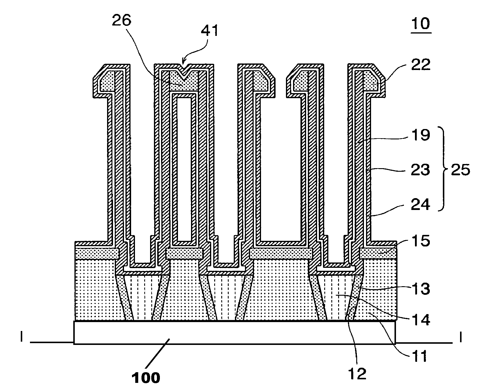
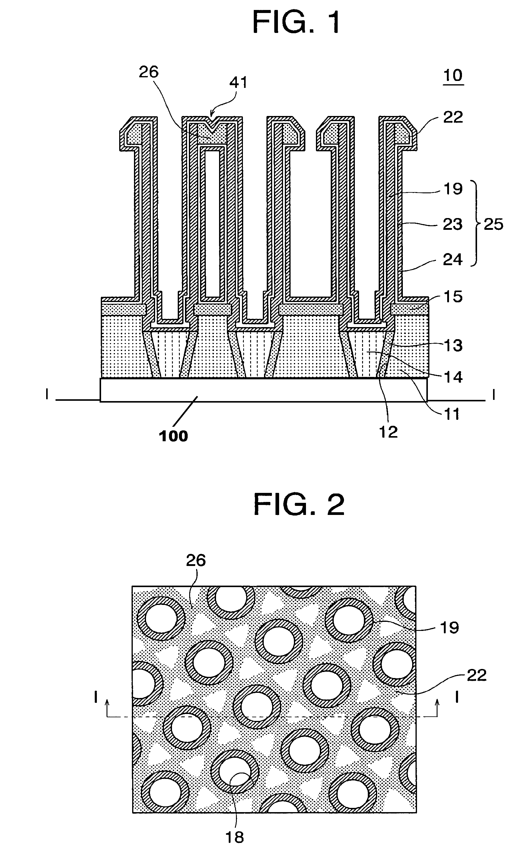
[0022]FIG. 1 shows a semiconductor device manufactured by a process according to an embodiment of the present invention. The semiconductor device 10 is configured as a DRAM device including MOS transistors (not shown) formed in the surface region of a semiconductor substrate 100 and an overlying structure shown in FIG. 1. The overlying structure shown in FIG. 1 includes an interlevel dielectric film 11, which overlies MOS transistors formed on the semiconductor substrate 100. The interlevel dielectric film 11 may include a plurality of insulation layers (not shown), between which bit lines are interposed. An etch stop film 15 configured by a silicon nitride film is disposed on the interlevel dielectric film 11.

[0023]The etch stop film 1...


PUM


Abstract

A method for forming a semiconductor device includes a plurality of crown-type capacitors in a capacitor-receiving insulating film, wherein bottom electrodes of the capacitors have an insulating spacer between each two of the bottom electrodes. The insulating spacer is formed by removing a hard mask used as an etching mask for forming cylindrical holes receiving therein capacitors including the bottom electrodes.

Description

[0001]This application is based upon and claims the benefit of priority from Japanese patent application No. 2006-187365, the disclosure of which is incorporated herein in its entirety by reference.BACKGROUND OF THE INVENTION[0002]1. Field of the Invention[0003]The present invention relates to a method for manufacturing a semiconductor device including a crown-type capacitor.[0004]2. Description of the Related Art[0005]Higher integration of memory cells has been desired in a semiconductor memory device, such as DRAM device (Dynamic Random Access Memory). In order to achieve the higher integration of the memory cells, it is necessary to increase the capacitance per the area which each cell capacitor of the memory cells occupies. One of the techniques for obtaining a higher capacitance for the cell capacitors is to form crown-type capacitors in the memory cell area. For forming the crown-type capacitors, a bottom electrode film is formed along the bottom and sidewall of cylindrical th...

Claims


Application Information

Patent Timeline
Patent Type & Authority Patents(United States)
IPC IPC(8): H01L21/20
CPCH01L27/10852H01L28/91H01L27/10894H10B12/09H10B12/033
Inventor ETO, TOYONORI
Owner MICRON TECH INC
Why Eureka
Try Eureka