Electronic parts board and method of producing the same

a technology of electronic components and parts, which is applied in the manufacture of capacitors, laminating printed circuit boards, other domestic articles, etc., can solve the problems of difficult to achieve a further reduction in the thickness of pre-set variable resistors, poor production efficiency, and high material cost, so as to facilitate the production of electronic components and reduce material costs , the effect of reducing production costs

Inactive Publication Date: 2010-06-01
TEIKOKU TSUSHIN IND CO LTD
View PDF10 Cites 14 Cited by
  • Summary
  • Abstract
  • Description
  • Claims
  • Application Information

AI Technical Summary

Benefits of technology

[0007]The present invention resides in a substrate for an electronic component that includes an insulating base and a flexible circuit board mounted on the insulating base, the flexible circuit board being a synthetic resin film provided thereon with terminal patterns and a conductor pattern whose surface is slidingly contacted with a slider, which is characterized in that the insulating base is a synthetic resin molded piece, and the flexible circuit board is insert-molded to the insulating base. According to this invention, the insulating base is made by molding a synthetic resin. Therefore, the production thereof is facilitated, and the material cost can be reduced in comparison to the ceramic substrate. It is also possible to achieve a reduction in thickness easily and at reduced cost. Further, because the flexible circuit board is insert-molded to the insulating base, the manufacture is facilitated. Further, the electronic component substrate can be mass-produced easily by simultaneously forming a large number of sets of conductor patterns on a synthetic resin film, and then simultaneously molding insulating bases together with respective flexible circuit boards provided with respective conductor patterns in each set, followed by cutting the integrally connected flexible circuit boards from each other, thereby enabling each individual discrete product to be obtained. Thus, productivity is improved.
[0008]A collector plate, provided with a tubular projection, is insert-molded to the insulating base in such a way that the tubular projection is positioned in through-holes respectively provided in the insulating base and the flexible circuit board. According to this invention, a collector plate provided with a tubular projection is insert-molded to the insulating base. Therefore, the insulating base and the collector plate can be integrated into one unit. Accordingly, it is possible to simplify the process of producing a rotating electronic component, e.g. a variable resistor, using the substrate for an electronic component.
[0009]The flexible circuit board is mounted on the insulating base by insert molding in a folded state so that the surface of the flexible circuit board is exposed on the upper and lower sides of the insulating base. According to this invention, the substrate for an electronic component can be easily fabricated into a chip.

Problems solved by technology

Therefore, the production efficiency is inferior, and the material cost is high.
Further, because the ceramic substrate is easily breakable, it has been difficult to achieve a further reduction in thickness of the pre-set variable resistor.

Method used


Image

  • Electronic parts board and method of producing the same
  • Electronic parts board and method of producing the same
  • Electronic parts board and method of producing the same

Examples


first embodiment

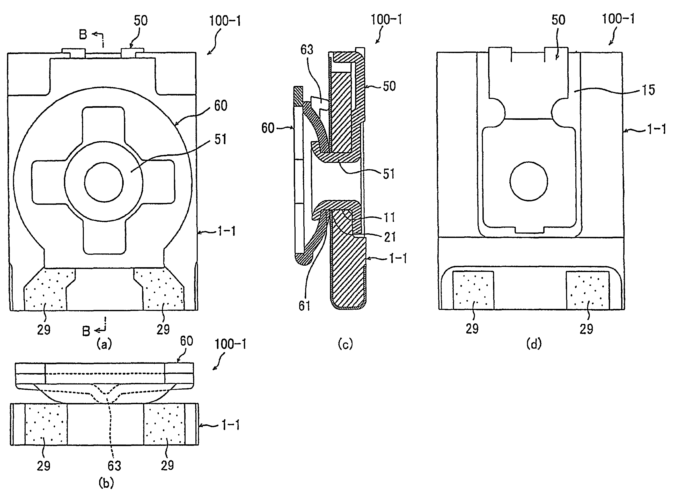
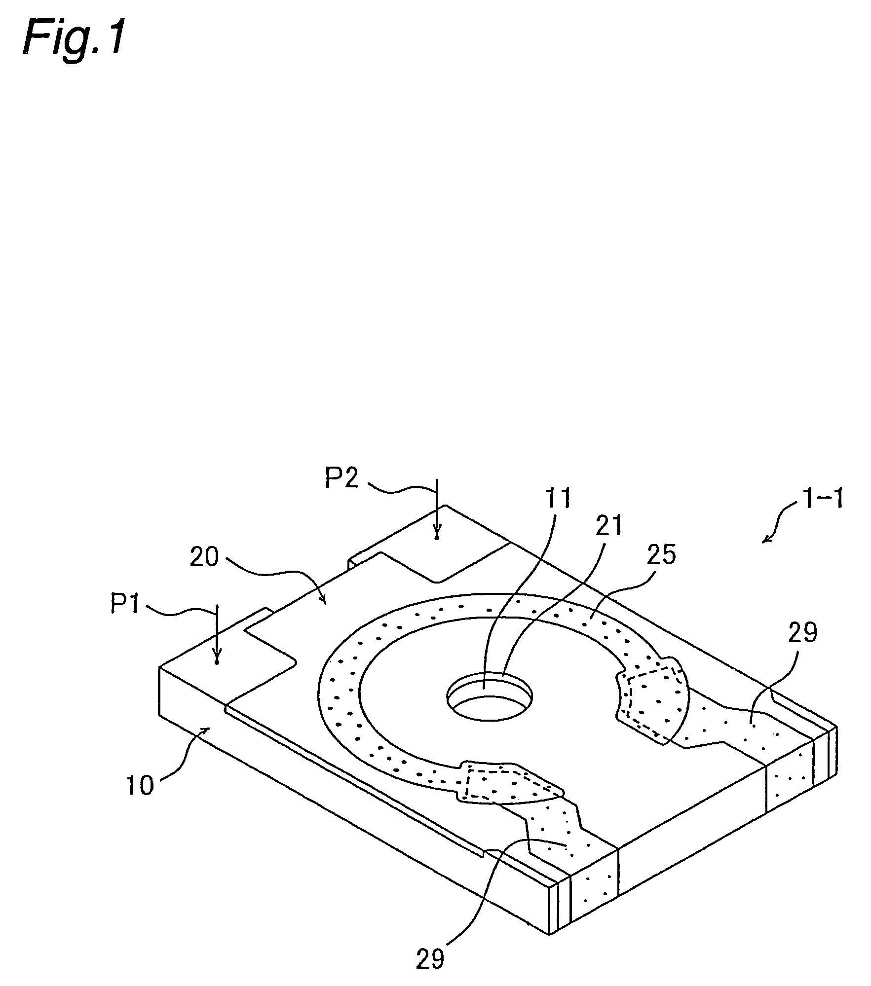
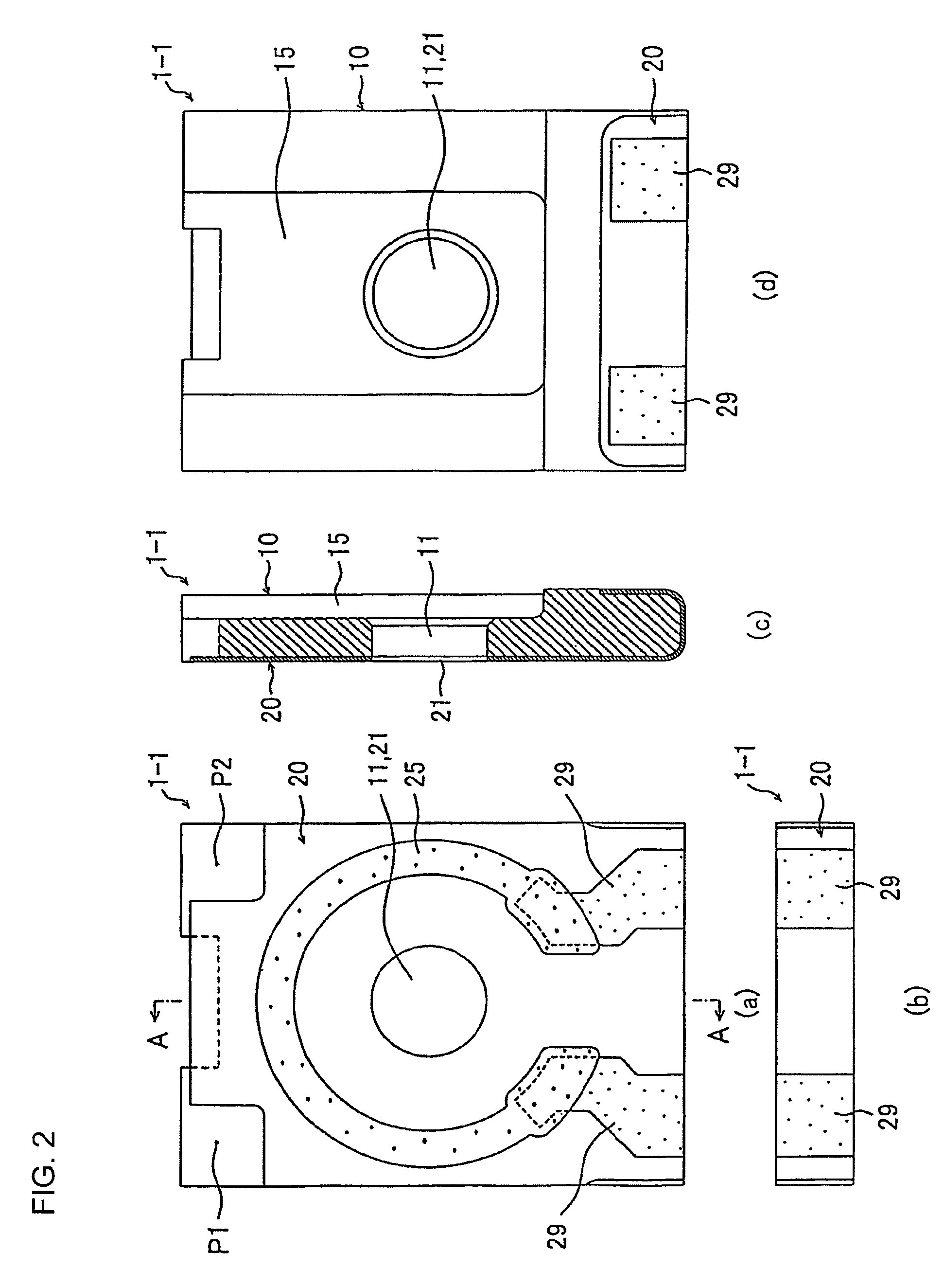
[0057]FIGS. 1 and 2 show a substrate 1-1 for an electronic component produced by using a first embodiment of the present invention. FIG. 1 is a perspective view. FIG. 2(a) is a plan view. FIG. 2(b) is a front view. FIG. 2(c) is a sectional view in the direction of arrows A-A in FIG. 2(a). FIG. 2(d) is a rear view. As shown in these figures, the electronic component substrate 1-1 includes an insulating base 10 and a flexible circuit board 20 integrally mounted on the insulating base 10 by insert molding. The electronic component substrate 1-1 will be described below for each constituent part thereof.

[0058]The insulating base 10 is an approximately rectangular plate-shaped synthetic resin molded piece provided in the center thereof with a circular through-hole 11. A collector plate accommodating recess 15 with a U-shaped sectional configuration is provided in the center of the lower side of the insulating base 10. The insulating base 10 is made of a thermoplastic synthetic resin, e.g....

second embodiment

[0070]FIG. 6 is a diagram showing an electronic component substrate 1-2 produced by using a second embodiment of the present invention. FIG. 6(a) is a plan view. FIG. 6(b) is a front view. FIG. 6(c) is a sectional view in the direction of arrows D-D in FIG. 6(a). FIG. 6(d) is a rear view. In the electronic component substrate 1-2 shown in these figures, the same portions as those of the electronic component substrate 1-1 are denoted by the same reference numerals, and a detailed description thereof is omitted. In the electronic component substrate 1-2 also, a flexible circuit board 20 is integrally mounted on the upper side of an insulating base 10 by insert molding. A resistor pattern 25 formed on the flexible circuit board 20 is made of a metal thin film deposited by physical vapor deposition or chemical vapor deposition.

[0071]The electronic component substrate 1-2 differs from the electronic component substrate 1-1 in that a collector plate 50-2 is also integrally molded in the i...

third embodiment

[0080]FIGS. 9 and 10 show an electronic component substrate 1-3 produced by using a third embodiment of the present invention. FIG. 9(a) is a perspective view as seen from above. FIG. 9(b) is a perspective view as seen from below. FIG. 10(a) is a plan view. FIG. 10(b) is a front view. FIG. 10(c) is a sectional view in the direction of arrows F-F in FIG. 10(a). FIG. 10(d) is a rear view. In the electronic component substrate 1-3 shown in these figures, the same portions as those of the electronic component substrates 1-1 and 1-2 are denoted by the same reference numerals, and a detailed description thereof is omitted. In the electronic component substrate 1-3 also, a flexible circuit board 20 is integrally mounted on the upper side of an insulating base 10 by insert molding. A resistor pattern 25 formed on the flexible circuit board 20 is made of a metal thin film deposited by physical vapor deposition or chemical vapor deposition. It should be noted that the constituent material of ...


PUM

PropertyMeasurementUnit
temperature coefficient of resistanceaaaaaaaaaa
flexibleaaaaaaaaaa

Abstract

An electronic component substrate (1-1) includes an insulating base (10) and a flexible circuit board (20) mounted on the insulating base (10). The flexible circuit board (20) is a synthetic resin film provided thereon with terminal patterns (29) and a conductor pattern (25) whose surface is slidingly contacted with a slider. The insulating base (10) is a synthetic resin molded piece. The flexible circuit board (20) is insert-molded to the insulating base (10). The electronic component substrate (1-1) is produced by preparing the flexible circuit board (20) and first and second mold members (41, 45) having a cavity (C1) with a shape that corresponds to the external shape of the electronic component substrate (1-1). Then, the flexible circuit board (20) is accommodated in the cavity (C1) between the first and second mold members (41,45), and the cavity (C1) is filled with a molten molding resin. After the molding resin has solidified, the first and second mold members (41, 45) are removed.

Description

BACKGROUND OF THE INVENTION[0001]1. Technical Field[0002]The present invention relates to a substrate for an electronic component that is usable for a pre-set variable resistor or the like, and also relates to a method of producing the electronic component substrate.[0003]2. Description of Related Art[0004]Conventionally, a chip type pre-set variable resistor has a ceramic substrate, a slider and a collector plate. The slider is installed on the upper side of the ceramic substrate, and the collector plate is installed on the lower side of the ceramic substrate. In fabrication, a tubular projection provided on the collector plate is inserted through a through-hole provided in the ceramic substrate and further through a fitting hole provided in the slider, and the distal end of the tubular projection is caulked, thereby rotatably securing the slider to the ceramic substrate. Rotating the slider causes a sliding contact provided on the slider to slide on the surface of a horseshoe-shap...

Claims


Application Information

Patent Timeline
Patent Type & Authority Patents(United States)
IPC IPC(8): H01C10/32H01C10/48H05K1/00H05K1/16H05K3/00
CPCB29C45/1418B29C45/14639H01C10/32H01C10/48B29C45/14467B29L2031/3406Y10T29/49082H05K1/0393H05K1/167H05K3/0014H05K3/0058Y10T428/24917
Inventor MIZUNO, SHINJIMITSUI, KOJIYANOSHITA, KATSUTOSHISUZUKI, SHINICHISHINOKI, TAKASHINAKAGOME, KAZUTAKAFUKUDA, NAOKIMORITA, KOZOMAKINO, DAISUKE
Owner TEIKOKU TSUSHIN IND CO LTD
Why Eureka
Try Eureka