Semiconductor device having stressed etch stop layers of different intrinsic stress in combination with PN junctions of different design in different device regions

a technology of etch stop layer and semiconductor device, which is applied in the direction of semiconductor device, transistor, electrical apparatus, etc., can solve the problems of increasing yield loss and instabilities in memory cells, and achieve enhanced pn junction profile, enhanced performance, and increased dislocation defects

Inactive Publication Date: 2010-06-08
TAIWAN SEMICON MFG CO LTD
View PDF12 Cites 0 Cited by
  • Summary
  • Abstract
  • Description
  • Claims
  • Application Information

AI Technical Summary

Benefits of technology

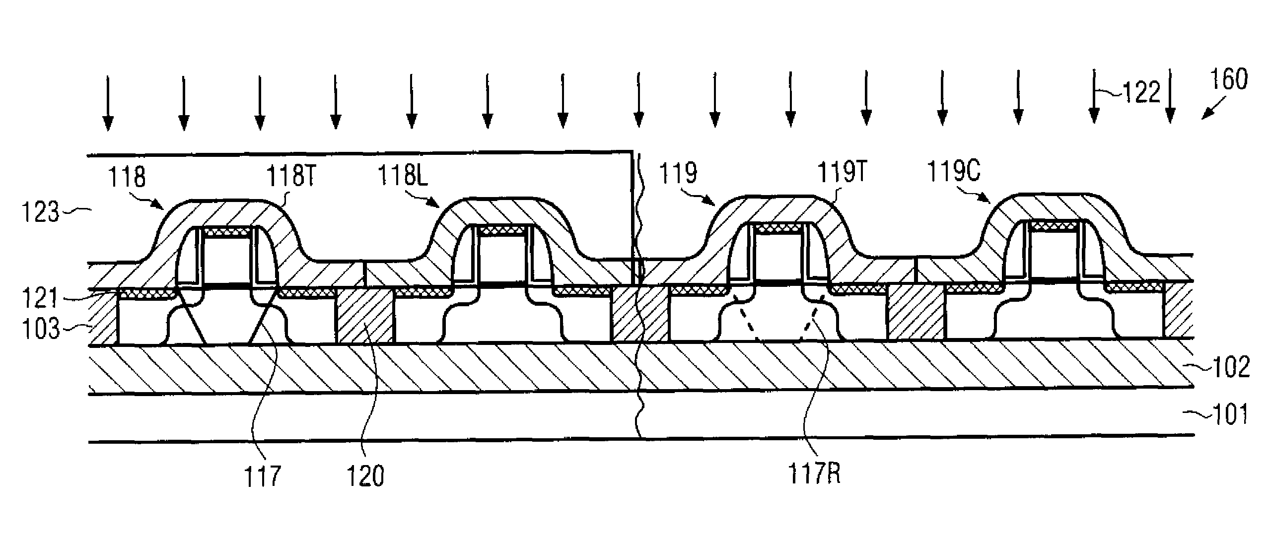
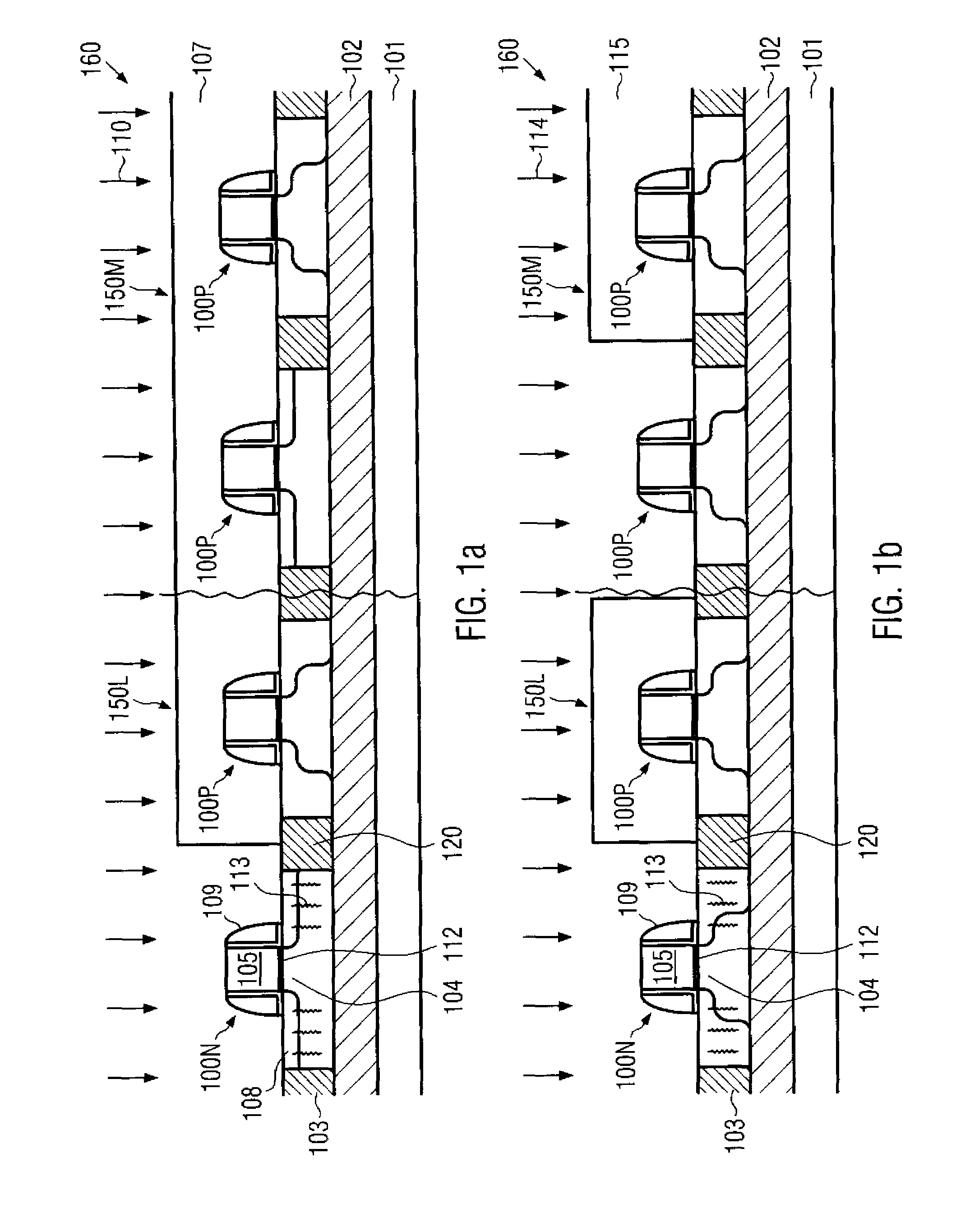
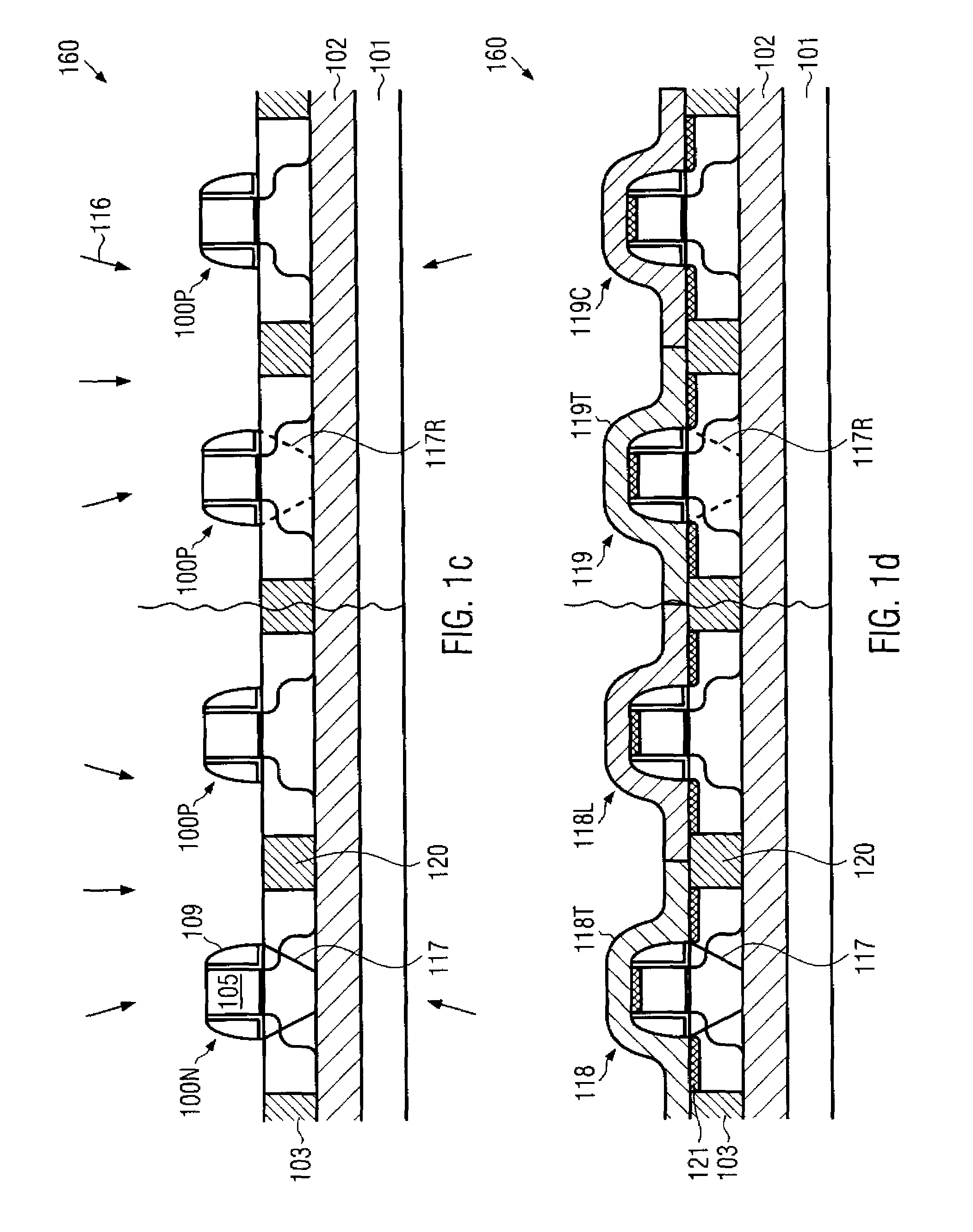
[0012]Generally, the present invention is directed to a technique for forming transistor elements of enhanced performance by combining enhanced PN junction profiles, obtained on the basis of a pre-amorphization process, and stressed overlayers, such as stressed contact etch stop layers, wherein the combination of these two techniques is performed in a highly local manner in a complex semiconductor device. It has been recognized that, in specific functional blocks of a complex integrated circuit, the interaction of the stressed overlayers and the increased dislocation defects caused by the pre-amorphization implantation may result in increased yield loss and instabilities in memory cells, such as static RAM areas of complex CPUs and other circuits having formed therein extended memory areas. Consequently, a high performance gain may be obtained in device areas, in which the interaction of stressed overlayers and increased dislocation defect rates in the drain and source regions and the body regions of the respective transistors may have little or no adverse effect on yield, while, in highly sensitive areas, such as static RAM areas, the “intensity” of at least the degree of defect generation, possibly in combination with a reduction of stress transfer, may be adjusted in order to obtain high performance in combination with a desired yield and stability of the corresponding functional block. For this purpose, the pre-amorphization implantation may be performed in a locally selective manner so as to provide substantially no pre-amorphization in the sensitive device areas or perform a respective pre-amorphization implantation on the basis of significantly reduced dose and / or energy in order to obtain a reduced dislocation defect rate after the re-crystallization. Consequently, the combined effect of stressed overlayers and more abrupt dopant gradients at the PN junctions may be adjusted in a local fashion so as to obtain overall performance gain as well as an increase in yield and reliability.

Problems solved by technology

It has been recognized that, in specific functional blocks of a complex integrated circuit, the interaction of the stressed overlayers and the increased dislocation defects caused by the pre-amorphization implantation may result in increased yield loss and instabilities in memory cells, such as static RAM areas of complex CPUs and other circuits having formed therein extended memory areas.

Method used


Image

  • Semiconductor device having stressed etch stop layers of different intrinsic stress in combination with PN junctions of different design in different device regions
  • Semiconductor device having stressed etch stop layers of different intrinsic stress in combination with PN junctions of different design in different device regions
  • Semiconductor device having stressed etch stop layers of different intrinsic stress in combination with PN junctions of different design in different device regions

Examples


Embodiment Construction

[0019]Illustrative embodiments of the invention are described below. In the interest of clarity, not all features of an actual implementation are described in this specification. It will of course be appreciated that in the development of any such actual embodiment, numerous implementation-specific decisions must be made to achieve the developers' specific goals, such as compliance with system-related and business-related constraints, which will vary from one implementation to another. Moreover, it will be appreciated that such a development effort might be complex and time-consuming, but would nevertheless be a routine undertaking for those of ordinary skill in the art having the benefit of this disclosure.

[0020]The present invention will now be described with reference to the attached figures. Various structures, systems and devices are schematically depicted in the drawings for purposes of explanation only and so as to not obscure the present invention with details that are well ...


PUM


Abstract

By selectively performing a pre-amorphization implantation process in logic areas and memory areas, the negative effect of the interaction between stressed overlayers and dislocation defects may be avoided or at least significantly reduced in the memory areas, thereby increasing production yield and stability of the memory areas.

Description

BACKGROUND OF THE INVENTION[0001]1. Field of the Invention[0002]Generally, the present invention relates to the formation of integrated circuits, and, more particularly, to the formation of field effect transistors in complex circuits including a complex logic circuitry and a memory area, such as a cache memory of a CPU.[0003]2. Description of the Related Art[0004]The fabrication of integrated circuits requires the formation of a large number of circuit elements on a given chip area according to a specified circuit layout. Generally, a plurality of process technologies are currently practiced, wherein, for complex circuitry, such as microprocessors, storage chips and the like, CMOS technology is currently the most promising approach, due to the superior characteristics in view of operating speed and / or power consumption. During the fabrication of complex integrated circuits using CMOS technology, millions of complementary transistors, i.e., N-channel transistors and P-channel transi...

Claims


Application Information

Patent Timeline
Patent Type & Authority Patents(United States)
IPC IPC(8): H01L29/80H01L21/336
CPCH01L21/26506H01L29/7843H01L21/84H01L27/1203H01L21/823807H01L21/823814
Inventor BLOOMQUIST, JOEJAVORKA, PETERHORSTMANN, MANFREDBURBACH, GERT
Owner TAIWAN SEMICON MFG CO LTD
Why Eureka
Try Eureka