Charged device model contact plate

a technology of charging device and contact plate, which is applied in the direction of short-circuit testing, air-break switches, instruments, etc., can solve the problems of a significant voltage overshoot and the primary threat of the thin gate oxide used in modern ic's, and achieve the effect of reducing parasitic inductance errors and increasing measurement errors

Active Publication Date: 2010-06-08
BARTH JON E +1
View PDF8 Cites 7 Cited by
  • Summary
  • Abstract
  • Description
  • Claims
  • Application Information

AI Technical Summary

Benefits of technology

[0011]Locating the connection of the 50 ohm impedance transmission line physically close to the DUT lead, pin, or contact minimizes parasitic inductance errors—which increases measurement errors. Such an arrangement insures that the measured very fast data is that of the Device Under Test (DUT), with minimal effect from parasitic inductance in the connection to the DUT contact being tested.

Problems solved by technology

While the conduction is increasing it produces a significant voltage overshoot, which is the primary threat to the thin gate oxides used in modern IC's.

Method used


Image

  • Charged device model contact plate
  • Charged device model contact plate

Examples


Embodiment Construction

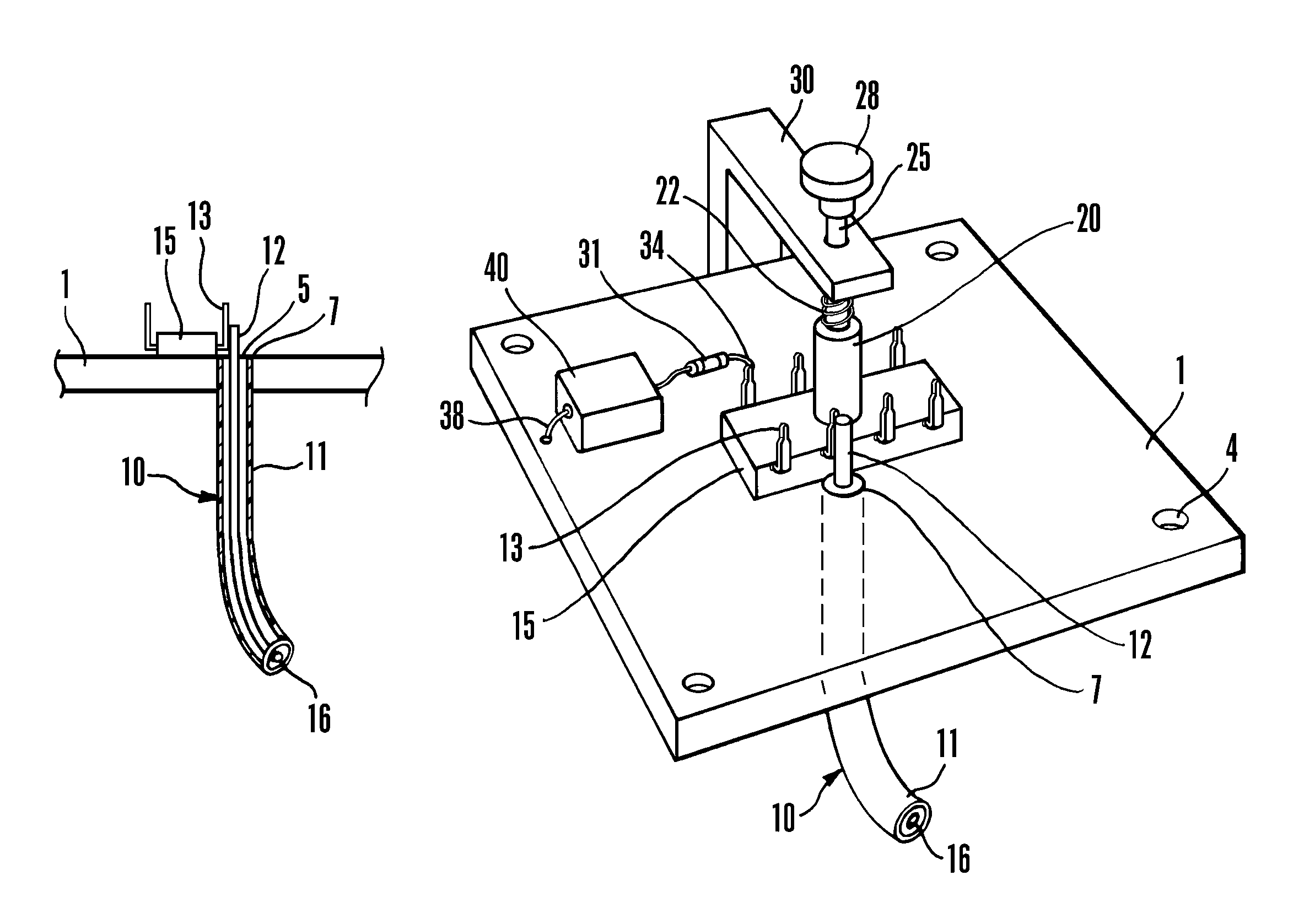
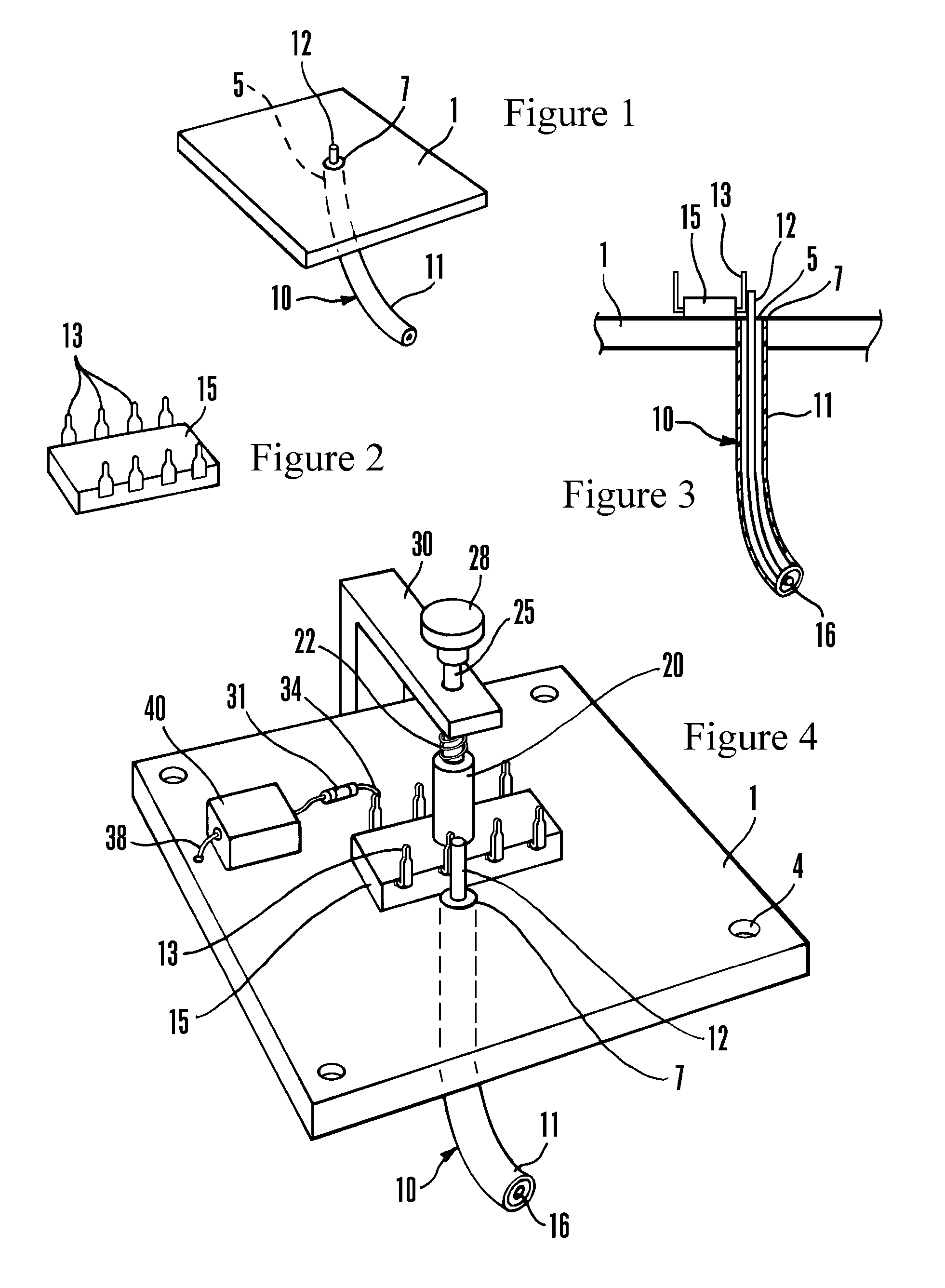
[0018]Reference is now made to the drawings wherein like numerals refer to like parts throughout. In FIG. 1, a metal ground plane 1 represents a physical and electrical reference. To maintain minimal parasitic inductance between an end 5 of a 50-ohm characteristic impedance coax 10, the end 5 is passed through an aperture 7 formed in the ground plane 1, and electrically connected to the metal ground plane 1 using solder or other commonly used methods of making electrical and physical connections between metals. The coax 10 consists of an outer conductor 11 and an inner conductor 12, the latter of which is shown projecting above the ground plane 1 in FIG. 1.

[0019]As is shown in FIG. 2, a plurality of conductive leads 13 extend from a DUT 15. To provide access to the plurality of leads 13, the DUT 15 is held down to the metal ground plane 1 in “dead bug style” (FIG. 3). The capacitance between the semiconductor chip and lead frame conductors inside the DUT 15 and the plurality of lead...


PUM


Abstract

A tester for applying very fast transmission line pulses (“VFTLP”) to select pins of a device under test (“DUT”), for example, an integrated circuit. The tester also provides for leakage measurement testing of the DUT after VFTLP testing. An end of a coaxial cable is received within an aperture formed in a metal ground plane. The outer conductor of the coaxial cable is attached to the metal ground plane and the inner conductor of the coaxial cable projects above an upper surface of the metal ground plane. A grip attached to the metal ground plane selectively retains the DUT upon the upper surface of the metal ground plane in a position placing a select pin in physical contact with the projecting inner conductor of the coaxial cable, completing the VFTLP circuit.

Description

CROSS-REFERENCE TO RELATED APPLICATION[0001]This application claims the benefit of U.S. Provisional Application Ser. No. 60 / 825,270, filed Sep. 11, 2006.TECHNICAL FIELD[0002]The present invention relates to an apparatus for Charged Device Model testing. More specifically, the present invention relates to a Very Fast Transmission Line Pulse (VFTLP) system for measuring current and voltage characteristics of an Integrated Circuit (IC) by establishing electrical connections between a VFTLP source and selected pins of the IC device under test (DUT).BACKGROUND ART[0003]Making Charged Device Model (CDM) type measurements on an integrated circuit (IC) with Very Fast TLP system test pulses requires a method to secure the IC in a location while making a low parasitic inductance electrical connection to one of its pins. The present specification describes a physical method to connect an electrical system to one pin of an IC and secure it while measuring its electrical parameters in sub-nanose...

Claims


Application Information

Patent Timeline
Patent Type & Authority Patents(United States)
IPC IPC(8): G01R31/02
CPCG01R1/0408G01R31/2886G01R31/025G01R31/52
Inventor BARTH, JON E.RICHNER, JOHN R.
Owner BARTH JON E
Why Eureka
Try Eureka