Lighting system

a technology of compact lighting and light source, which is applied in the field of compact lighting system, can solve the problems of uneven illumination, high cost, and increase the manufacturing cost of semiconductor light emitting modules, and achieve the effect of facilitating the cleaning of the filter surfa

Inactive Publication Date: 2010-06-15
YANCHERS CORP
View PDF16 Cites 98 Cited by
  • Summary
  • Abstract
  • Description
  • Claims
  • Application Information

AI Technical Summary

Benefits of technology

[0012]According to the lighting system of the present invention, since all lights emitted from the semiconductor light emitting devices are led to the same location in such a manner as to be mutually superposed, the lighting system can illuminate a predetermined spatial region in an extremely high luminance. In addition, even if luminance unevenness occurs in each semi conductor light emitting device itself, since all lights are led to the same location, the influence of each semiconductor light emitting device itself does not occur at all. Therefore, a plurality of semiconductor light emitting devices having a lot of variations in luminance can be used without selection thereof, and particularly an effective use of a power LED having a low manufacturing yield is possible. Even if one of the plurality of the semiconductor light emitting devices does not emit light due to any cause, the illumination in the illumination region is just lowered by the corresponding amount. Accordingly, this lighting system of the present invention is extremely convenient in a state where the lighting system can not be replaced.
[0021]The plurality of the plano-convex lenses may be integrally molded in an array. In this case, positioning of the plano-convex lens to each semiconductor light emitting device is extremely easily made, thus easily manufacturing a lighting system.

Problems solved by technology

Accordingly, in a case where this power LED is used as a light source for illumination requiring a uniform luminous distribution characteristic, it leads to an extremely high cost due to the low manufacturing yield as described above.
Therefore, as a result of basically eliminating use of a light emitting diode device exceeding a predetermined tolerance, the manufacturing yield of light emitting diodes deteriorates in the same way as in the case of the power LED, leading to an increase of a manufacturing cost of the semiconductor light emitting module.
Therefore, there occurs illumination unevenness in response to the variation in light emitting luminance of the individual LED chip.
Accordingly, this light emitting device is not nearly practical in terms of costs.
As a result, in the same way as in the case of Japanese Patent Application Laid-open No. 2002-049326, the variation in the light emitting luminance of each light emitting diode leads directly to illumination unevenness in the illumination region, so that the uniform luminous distribution characteristic, i.e., the uniform illumination distribution can not be basically obtained.
In addition, in a case of selecting the light emitting diodes for avoiding this problem, the manufacturing cost increases.

Method used


Image

  • Lighting system
  • Lighting system
  • Lighting system

Examples


Embodiment Construction

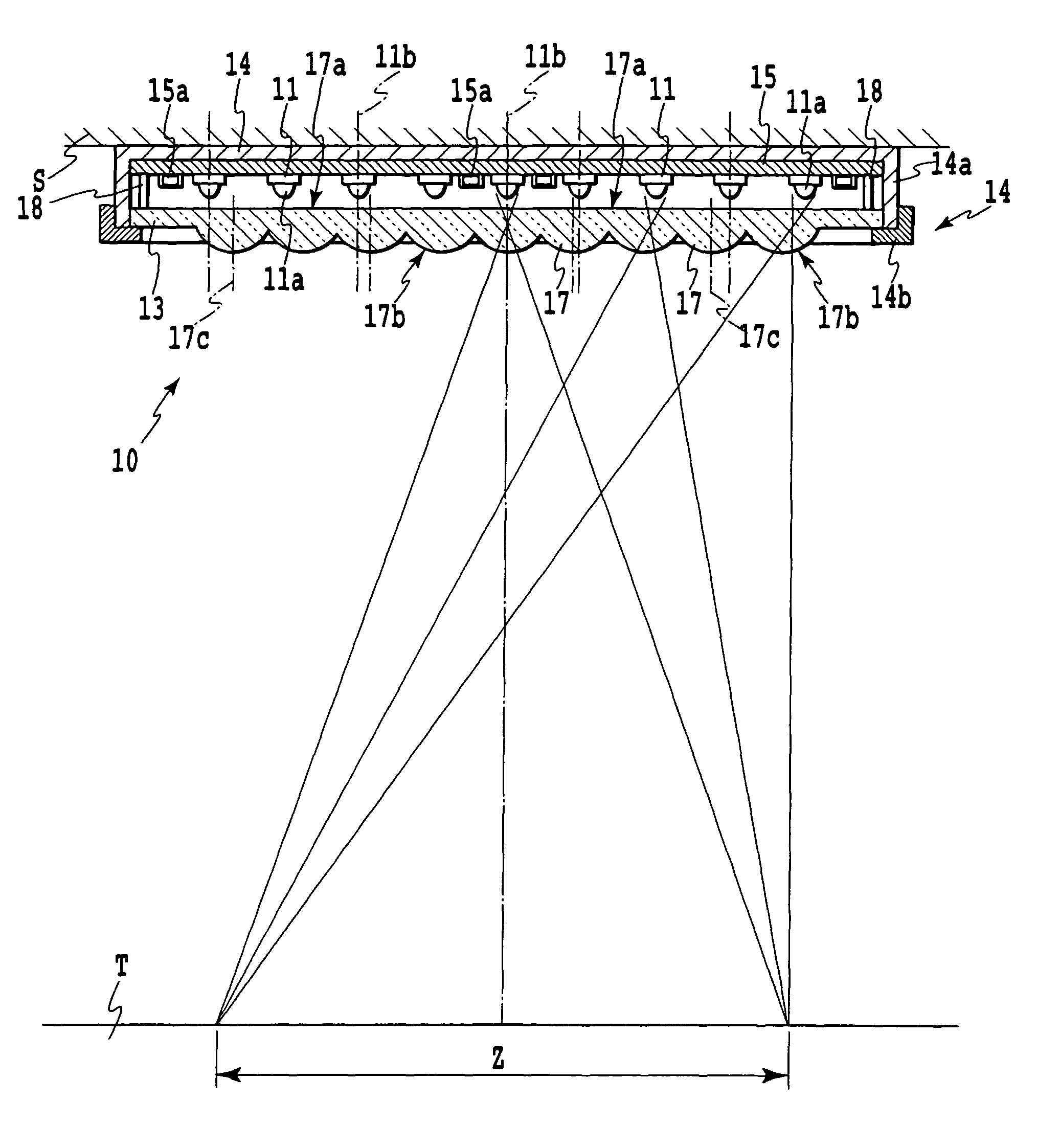
[0032]A lighting system in an embodiment of the present invention will be described in detail with reference to FIGS. 2 to 6. The present invention is, however, not limited to the embodiment, but can include all alternations and modifications included in the concept of the present invention described in claims. Accordingly, it is apparent that the present invention can be applied to any other technology within the spirit thereof.

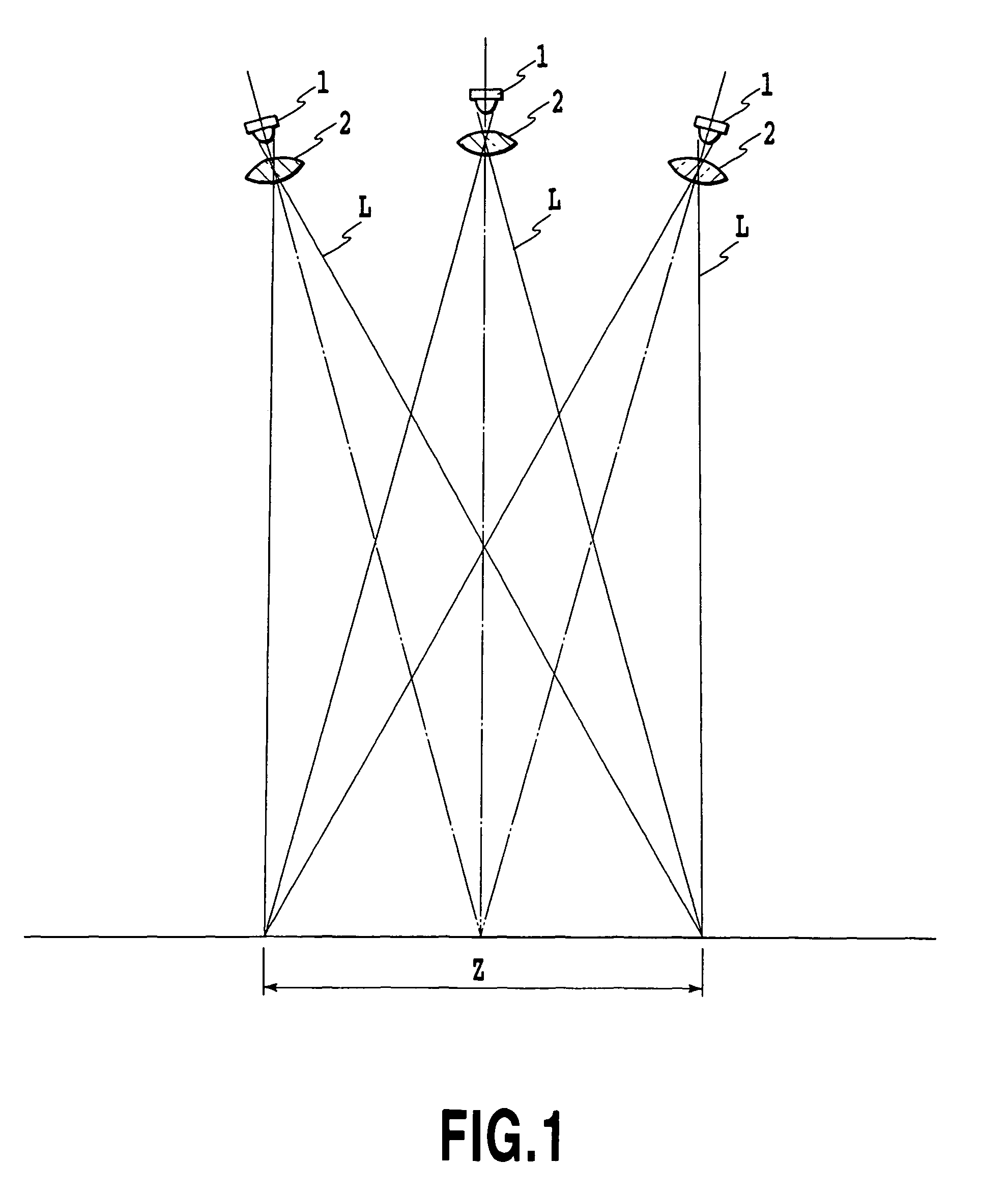
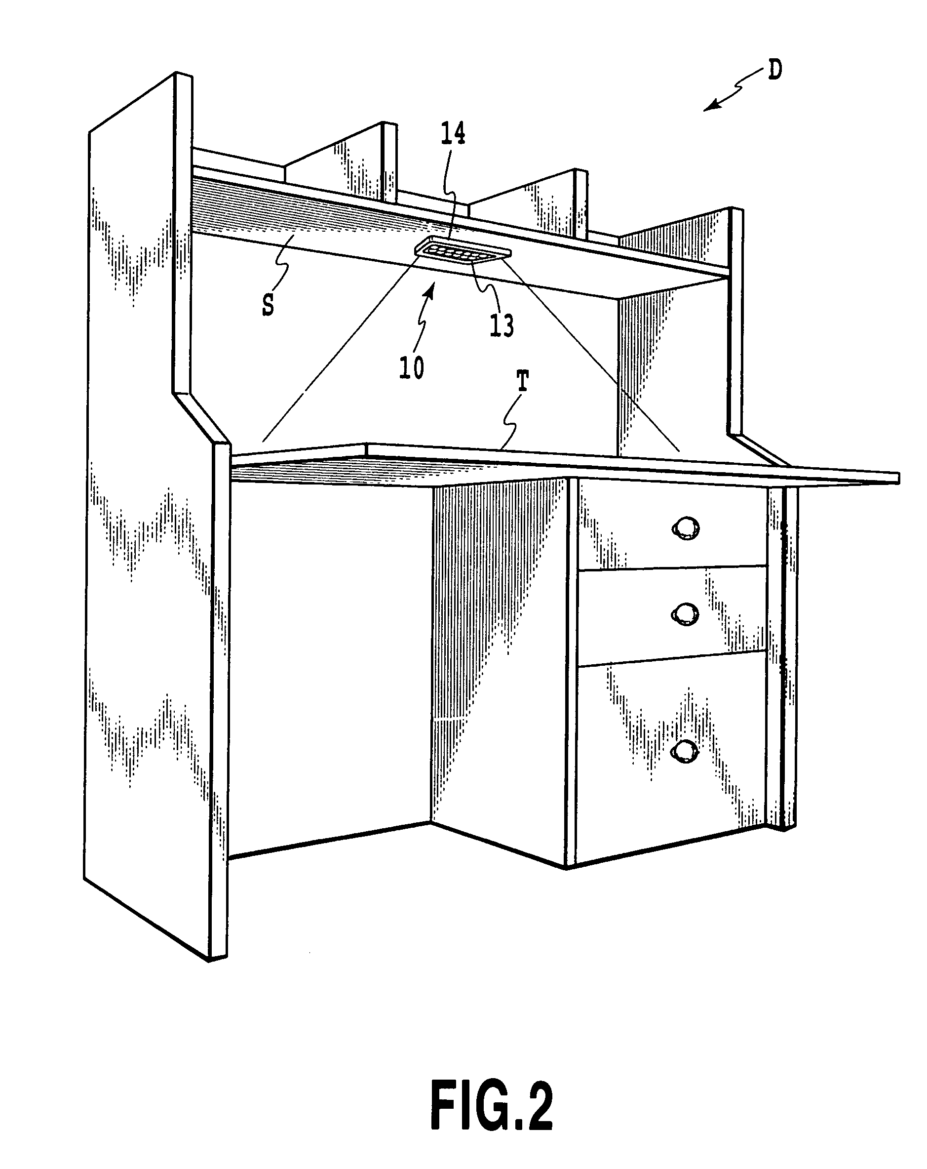
[0033]FIG. 2 shows an outside appearance in an embodiment where the present invention is applied to a reading lamp incorporated into a study desk, FIG. 3 shows a cross-sectional structure thereof and FIG. 4 shows an exploded state of an outside appearance of a main part thereof. A reading lamp 10 in the embodiment is mounted on the back side of the shelf board S of a writing desk D and designed to illuminate on a top board T. The reading lamp 10 has a main part composed of a LED module into which a plurality of LED chips 11 are incorporated in a predetermine...


PUM


Abstract

The lighting system according to the present invention includes an electrical wiring substrate in which a connector to a power source is formed, a plurality of LED chips mounted in a predetermined array pattern on the electrical wiring substrate, a deflection lens array disposed in proximity to the LED chips between the LED chip and the predetermined illumination region and a housing for receiving the electrical wiring substrate and the deflection lens array. A plurality of deflection lenses are integrally molded in the deflection lens array to lead lights from the LED chips to the predetermined illumination region in a state where the lights from the LED chips are superposed with each other. The lights emitted from the LED chips are collected in a state where they all are superposed in a common, single illumination region through the deflection lenses.

Description

BACKGROUND OF THE INVENTION[0001]1. Field of the Invention[0002]The present invention relates to a compact lighting system having a high illumination and a uniform luminous distribution characteristic.[0003]2. Description of the Related Art[0004]A light emitting diode (LED) has an advantage that it is compact and the power consumption is small and therefore, the lifetime is more than ten times that of a fluorescent light. Incorporation of a condenser lens into this LED allows approximately 90% of the emitted lights to be projected ahead without an additional, specific reflector. This type of lighting system can project light having extremely strong directivity and high luminance. There is developed a large-sized LED (power LED) a light emitting area of which is larger than conventional and which has extremely high luminance. There are studies on an application of such a power LED in various fields as a compact light source for illumination in low consumption power instead of a conve...

Claims


Application Information

Patent Timeline
Patent Type & Authority Patents(United States)
IPC IPC(8): F21V5/00
CPCF21S8/026F21V5/04F21V13/02F21V5/003F21S8/04F21V29/763F21V29/004F21W2131/301F21W2131/304F21W2131/402F21Y2101/02F21Y2103/003F21Y2105/001F21Y2113/005F21V9/00F21V29/89F21Y2103/10F21Y2105/10F21Y2113/13F21Y2115/10
Inventor SHIMADA, JUNICHIKAWAKAMI, YOICHIYAMADA, MOTOKAZUKATO, MASARU
Owner YANCHERS CORP
Why Eureka
Try Eureka