Trench junction barrier controlled Schottky device with top and bottom doped regions for enhancing forward current in a vertical direction

a technology of vertical direction and doped regions, applied in the direction of semiconductor devices, electrical equipment, transistors, etc., can solve the problems of increasing production costs, affecting and other problems, and achieve the effect of greatly improving the utilization rate of silicon area

Active Publication Date: 2010-06-15
ALPHA & OMEGA SEMICON LTD
View PDF18 Cites 17 Cited by
  • Summary
  • Abstract
  • Description
  • Claims
  • Application Information

AI Technical Summary

Benefits of technology

[0009]It is therefore an aspect of the present invention to provide a new and improved Schottky diode with the junction barrier metal deposited in the trenches with dopant regions for preventing the reverse leakage current disposed on the sidewalls of the trenches and at surrounding the top and bottom corners of the trenches. The depletion from the PN junctions provides the function to shield the Schottky barrier from the reverse voltage. The silicon area utilization is greatly improved and the requirement of a round trench bottom is eliminated such that the above discussed limitations and difficulties of the convention Schottky is resolved.
[0011]Another aspect of this invention is to provide new and improved Schottky device configuration that in addition to improve the silicon area utilization of the junction barrier Schottky (JBS) by forming the Schottky junction on the sidewall of trench, the junction barrier Schottky (JBS) formed along the trench sidewalls is combined and integrated with either planar or trenched MOSFET devices to improved the performances of the semiconductor power devices.
[0012]Another aspect of this invention is to provide new and improved Schottky device configuration that in addition to improve the silicon area utilization of the junction barrier Schottky UBS) by forming the Schottky junction on the sidewall of trench, the Schottky device is now manufactured with simplified manufacturing processes with reduced process complexity. Furthermore, the simplified manufacturing processes are implemented with standard processing steps as that commonly implemented for typical MOSFET power device manufacture thus greatly reduce the production cost and can be conveniently combined and integrated with a standard MOSFET device.

Problems solved by technology

The trench Schottky diode configuration leads to another technical difficulty due to the breakdown vulnerability at trench corners where there are sharp edges.
In order to overcome such difficulties, a round trench bottom is necessary and that causes the production cost to increase.
Due to these reasons, a person of ordinary skill in the art of designing and manufacturing devices including Schottky diodes is still confronted with the technical difficulties and limitations that a reduction of production cost cannot easily achieved.
Low Schottky barrier height will give rise to higher leakage current in the reverse blocking operation of the diode.
The disadvantage of the JBS is the reduced Schottky surface area from the p-type junctions.
The rounding of the sharp corners requires extra process steps and specialized equipment and all these requirements cause an increase in the production costs.

Method used


Image

  • Trench junction barrier controlled Schottky device with top and bottom doped regions for enhancing forward current in a vertical direction
  • Trench junction barrier controlled Schottky device with top and bottom doped regions for enhancing forward current in a vertical direction
  • Trench junction barrier controlled Schottky device with top and bottom doped regions for enhancing forward current in a vertical direction

Examples


Embodiment Construction

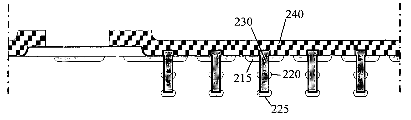
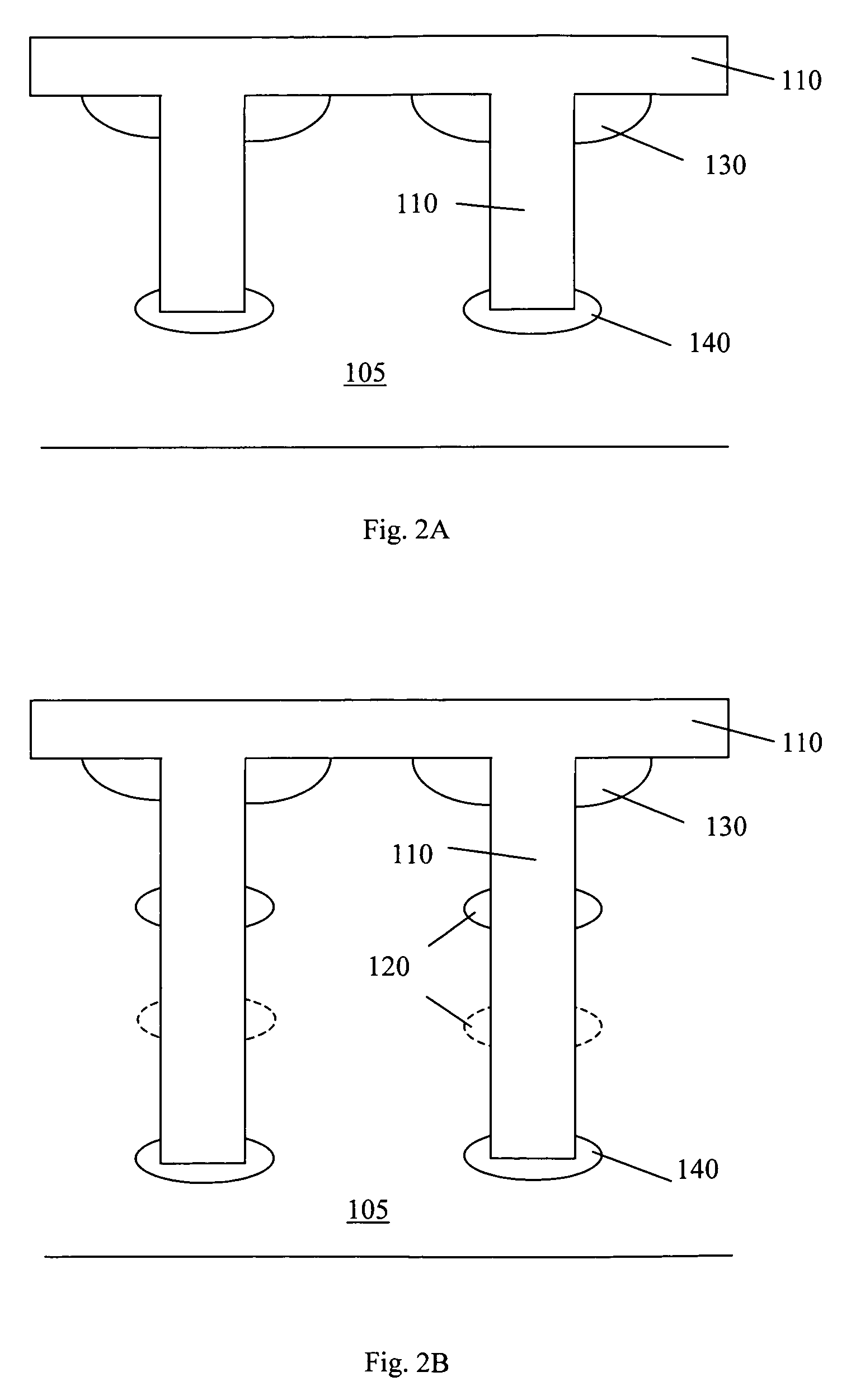
[0023]Referring to FIG. 2A for a cross sectional view of an Schottky diode 100 of this invention. The Schottky diode 100 is supported and formed in a semiconductor substrate, e.g., a N-doped silicon substrate 105. The Schottky diode 100 includes a plurality of trenches forming a plurality of semiconductor mesas. In the preferred embodiment as shown in FIG. 2A the trenches are filled with Schottky barrier metal, e.g., Ti / TiN or Tungsten metal 110. In another preferred embodiment (not shown), at least a portion of vertical surface of semiconductor mesas is lined with Schottky barrier metal. For the purpose of preventing leakage current generated by the reverse voltage, P-dopant regions 130 are formed on the mesas surrounding the top portions of the trenches and P-dopant regions 140 are formed that surrounding the bottom of the trenches.

[0024]As shown in FIG. 2A, P-dopant regions 130 are formed on the top corners of mesas without extending over the whole top surface of mesas. Schottky ...


PUM


Abstract

A Schottky diode includes at least a trenched opened in a semiconductor substrate doped with a dopant of a first conductivity type wherein the trench is filled with a Schottky junction barrier metal. The Schottky diode further includes one or more dopant region of a second conductivity type surrounding sidewalls of the trench distributed along the depth of the trench for shielding a reverse leakage current through the sidewalls of the trench. The Schottky diode further includes a bottom-doped region of the second conductivity type surrounding a bottom surface of the trench and a top-doped region of the second conductivity type surrounding a top portion of the sidewalls of the trench. In a preferred embodiment, the first conductivity type is a N-type conductivity type and the middle-depth dopant region comprising a P-dopant region.

Description

[0001]This Patent Application is a Continuation in Part (CIP) Application of a Application with a Ser. No. 11 / 056,346 filed by a common Inventor of this Application on Feb. 11, 2005 now U.S. Pat. No. 7,285,822. The Disclosures made in that Application is hereby incorporated by reference.BACKGROUND OF THE INVENTION[0002]1. Field of the Invention[0003]The invention relates generally to the semiconductor power devices. More particularly, this invention relates to an improved and novel manufacturing process and device configuration for providing the MOSFET device with shielded trench gates with cells provided with Schottky source contact for improving performance of high frequency power switching, H-bridge and synchronization rectification applications.[0004]2. Description of the Related Art[0005]As the applications of Schottky diodes become more widespread, particularly for reducing the power consumption and increasing the switching speed, it becomes even more important to improve the ...

Claims


Application Information

Patent Timeline
Patent Type & Authority Patents(United States)
IPC IPC(8): H01L29/47H01L29/872
CPCH01L29/407H01L29/66727H01L29/66143H01L29/7811H01L29/782H01L29/8725H01L29/66734H01L29/0623H01L29/1095
Inventor LUI, SIK KBHALLA, ANUP
Owner ALPHA & OMEGA SEMICON LTD
Why Eureka
Try Eureka