Hybrid Schottky source-drain CMOS for high mobility and low barrier

a technology of source-drain cmos and high mobility, applied in the field of semiconductor fabrication, can solve the problems of significant degrading the drive current of a schottky cmos, many challenges facing the integration of schottky s/d technology, and the failure of material integration, etc., and achieve the effect of lowering nmos and pmos schottky barriers

Active Publication Date: 2010-06-15
TAIWAN SEMICON MFG CO LTD
View PDF13 Cites 15 Cited by
  • Summary
  • Abstract
  • Description
  • Claims
  • Application Information

AI Technical Summary

Benefits of technology

[0008]Alternative embodiments further include a CMOS device. The CMOS device comprises a substrate, the substrate having a first region and a second region, the first region having a first crystal orientation, the second region having a second crystal orientation, wherein the first crystal orientation is different from the second crystal orientation. Alternative embodiments comprise an NMOSFET formed on the first region, the NMOSFET comprising an NMOS source electrode, an NMOS drain electrode, and a Schottky contact formed with at least one of the NMOS source electrode and the NMOS drain electrode; and a PMOSFET formed on the second region; the PMOSFET comprising a PMOS source electrode, a PMOS drain electrode, and a Schottky contact formed with at least one of the PMOS source electrode and the PMOS drain electrode.

Problems solved by technology

Despite these clear advantages, there are many challenges facing the integration of Schottky S / D technology with current manufacturing methods.
For example, a large Schottky barrier at a source electrode can significantly degrade the drive current of a Schottky CMOS.
However, such material integration has not always been successful.

Method used


Image

  • Hybrid Schottky source-drain CMOS for high mobility and low barrier
  • Hybrid Schottky source-drain CMOS for high mobility and low barrier
  • Hybrid Schottky source-drain CMOS for high mobility and low barrier

Examples


Embodiment Construction

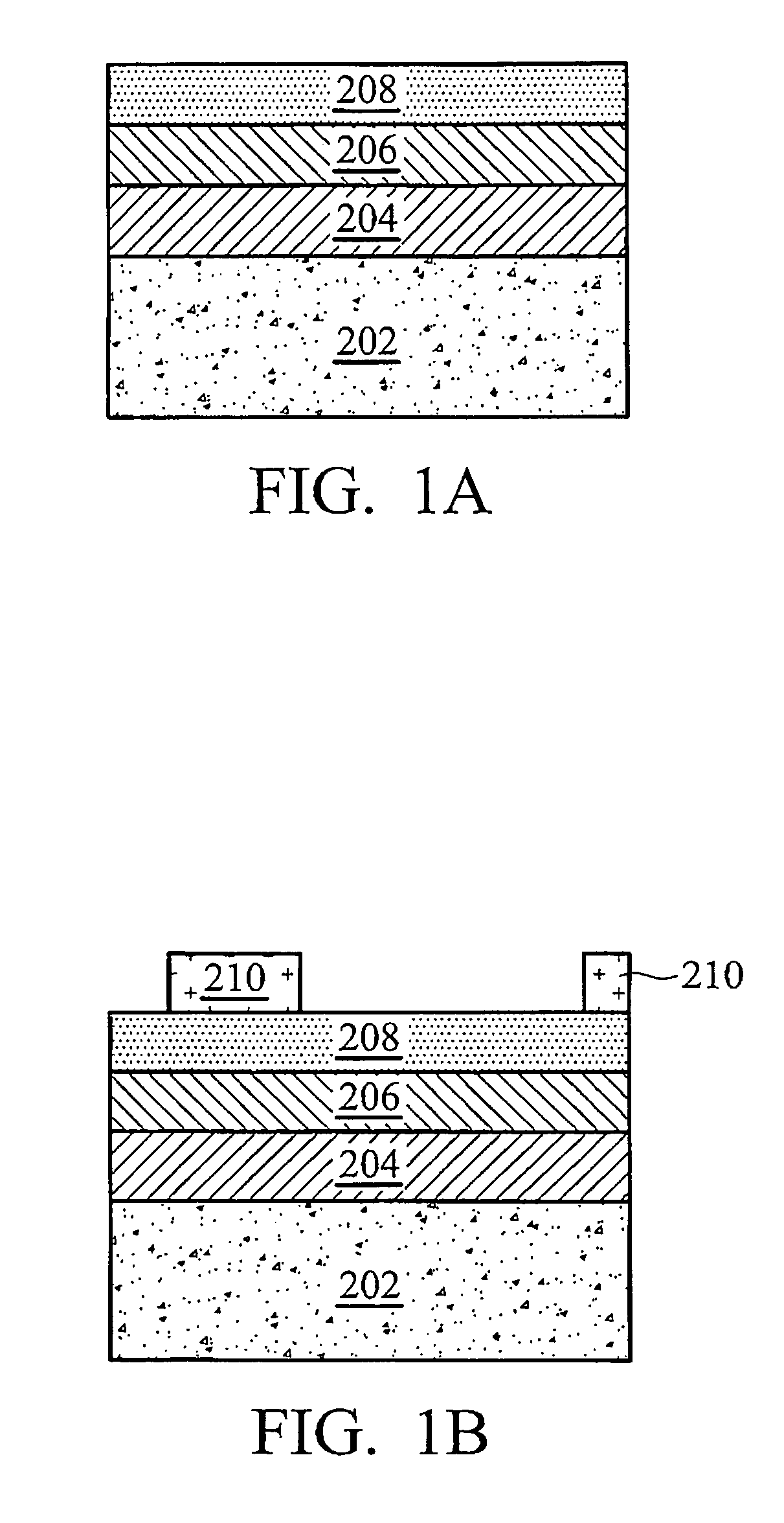
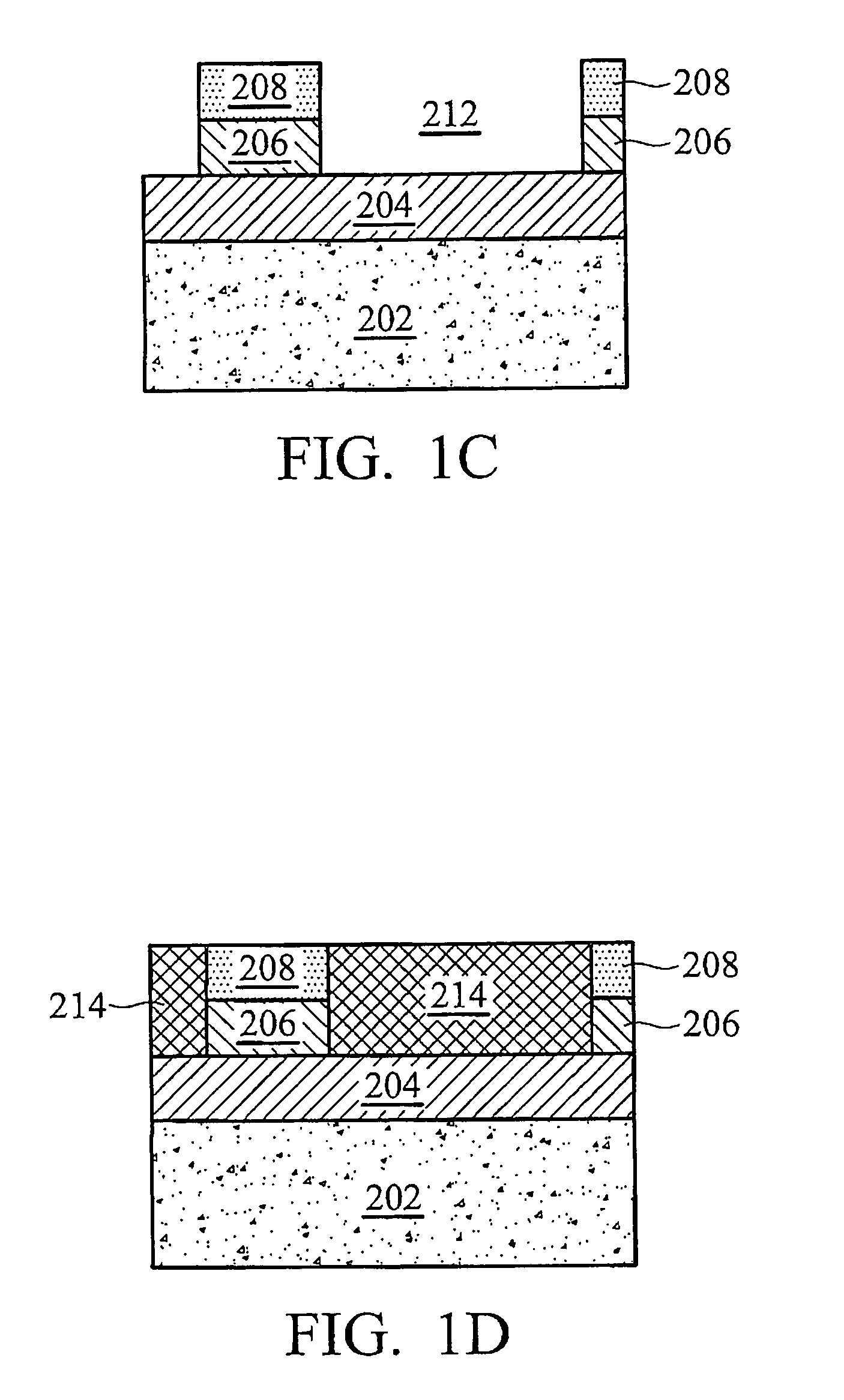
[0019]The making and using of the presently preferred embodiments are discussed in detail below. It should be appreciated, however, that the present invention provides many applicable inventive concepts that may be embodied in a wide variety of specific contexts. The specific embodiments discussed are merely illustrative of specific ways to make and use the invention, and do not limit the scope of the invention.

[0020]When a metal contacts a semiconductor, a barrier forms at the metal-semiconductor interface. The barrier (or barrier height) depends on the work function difference between the metal and the semiconductor, the interface state density, and the doping level in the semiconductor. In the absence of surface states, the barrier height is mainly determined by the work function difference between the metal and the semiconductor. If there is a large density of surface states, the barrier height is determined by the semiconductor surface, and it is independent of the metal work f...


PUM


Abstract

A CMOS device is provided. A semiconductor device comprises a substrate, the substrate having a first region and a second region, the first region having a first crystal orientation represented by a family of Miller indices comprising {i,j,k}, the second region having a second crystal orientation represented a family of Miller indices comprising {l,m,n}, wherein l2+m2+n2>i2+j2+k2. Alternative embodiments further comprise an NMOSFET formed on the first region, and a PMOSFET formed on the second region. Embodiments further comprise a Schottky contact formed with at least one of a the NMOSFET or PMOSFET.

Description

TECHNICAL FIELD[0001]This invention relates generally to semiconductor fabrication and more particularly to a fabrication method for a complimentary metal oxide semiconductor (CMOS) device having metal-semiconductor, source / drain junctions.BACKGROUND[0002]A common electrical contact used in modem devices is the metal-semiconductor contact. Depending on the materials, the contact may be ohmic or rectifying. An ohmic contact has low electrical resistance, regardless of the direction of current flow. A rectifying contact behaves as a diode in that it conducts current freely in one direction but has a barrier to current flow in another. This so-called Schottky barrier is the potential necessary for an electron to pass from the metal to the semiconductor, and it is an important parameter in determining the electrical properties of the metal-semiconductor contact.[0003]Recently, advanced semiconductor devices use a metal-semiconductor, Schottky contact to form the source and / or drain of a...

Claims


Application Information

Patent Timeline
Patent Type & Authority Patents(United States)
IPC IPC(8): H01L29/04
CPCH01L21/823807H01L21/823821H01L21/823878H01L21/8252H01L27/1207H01L21/84H01L27/0922H01L27/1203H01L21/8258H01L29/785
Inventor KE, CHUNG-HUKO, CHIH-HSINCHEN, HUNG-WEILEE, WEN-CHINCHI, MIN-HWA
Owner TAIWAN SEMICON MFG CO LTD
Why Eureka
Try Eureka