Radiation imaging device with irregular rectangular shape and extraoral dental imaging system therefrom

a radiation imaging and rectangular shape technology, applied in the field of digital radiation imaging, can solve the problems of crystal edge cracks or fractures, detector elements are much more vulnerable to damage, and the signal collecting electric field applied to the crystals is affected by distortions, so as to save material costs, speed up data readout, and efficient beam coverage

Inactive Publication Date: 2010-06-22
OY AJAT LTD
View PDF38 Cites 13 Cited by
  • Summary
  • Abstract
  • Description
  • Claims
  • Application Information

AI Technical Summary

Benefits of technology

[0011]An important aspect of the invention is that the shape of the active area of the sensor is made to match as exactly as possible the X-ray beam shape (or shapes) of a specific application. If the X-ray beam shape differs significantly from a cone or a fan beam shape or if the application requires the use of two or more X-ray beams with different shapes no conventional sensor of linear or rectangular shape will match effectively the X-ray beam shapes. For example, in an application using a fan beam and a rectangular cone beam for different imaging modes a sensor with irregular shape of active area provides much more efficient beam coverage than a conventional sensor with a large rectangular active area. The benefits of an optimized sensor area include savings in material costs, faster data readout and the possibility to use one sensor instead of many for different beam shapes.
[0012]Another aspect of the invention is the method of manufacturing the mosaic like sensor structure by leaving a finite physical gap between adjacent detector elements. This structure is a departure from the prior art teachings of eliminating dead space between individual detector chips. This inventive manufacturing method of not providing minimum dead space within the active imaging area brings definite advantages in terms of production yield and long term endurance of the sensor. Since solid state semiconductors are generally fragile crystals, mounting them in physical contact increases greatly the risk of damaging the crystal edges with cracks or fractures during production. It also leaves the detector elements much more vulnerable to damage caused by thermal expansion or mechanical shock compared to the method of mounting the elements with an intermediate physical gap. Moreover, physical contact between the semiconductor detector crystals can lead to distortions in the signal collecting electric field applied to the crystals. The gap between the detector elements may be simply empty space or the gap may be created by placing some material such a mylar film in between the detector elements. The size of the gap is preferably but not necessary equal to or a multiple of the pixel size of the detector elements.
[0013]Still another aspect of the invention is the effective method of manufacturing several different mosaic type sensors with active areas of dissimilar irregular shape on identical sensor substrates the substrate being generally a printed circuit board (PCB). Since the control and signal readout schemes of the separate detector elements are identical it is possible to design one PCB to accommodate different combinations of detector elements. Thus with one type of a PCB and one (or more) type of a detector element, sensors with various shapes of active area for different applications can be produced easily and without the need of any costly and time consuming design changes of the substrate. Alternatively, a desired shape of the active sensor area can be constructed by combining side by side two or more separate either identical or non-identical sensor substrates each substrate populated with one or more detector elements of either similar or dissimilar size or shape.

Problems solved by technology

Since solid state semiconductors are generally fragile crystals, mounting them in physical contact increases greatly the risk of damaging the crystal edges with cracks or fractures during production.
It also leaves the detector elements much more vulnerable to damage caused by thermal expansion or mechanical shock compared to the method of mounting the elements with an intermediate physical gap.
Moreover, physical contact between the semiconductor detector crystals can lead to distortions in the signal collecting electric field applied to the crystals.

Method used


Image

  • Radiation imaging device with irregular rectangular shape and extraoral dental imaging system therefrom
  • Radiation imaging device with irregular rectangular shape and extraoral dental imaging system therefrom
  • Radiation imaging device with irregular rectangular shape and extraoral dental imaging system therefrom

Examples


Embodiment Construction

[0025]A inventive radiation imaging device includes plural individual detectors defining an irregular rectangular active area responsive to x-rays and with different widths along a length of the active area. The individual detectors may be of different rectangular shapes and mounted on a motherboard. The motherboard may be formed of a first module mounting a first of two individual detectors and a second module detachable connected to the first module and mounting a second of two individual detectors.

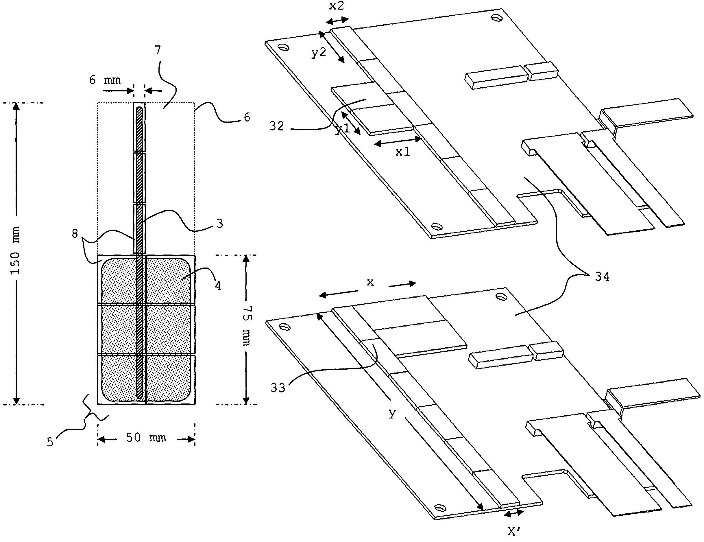
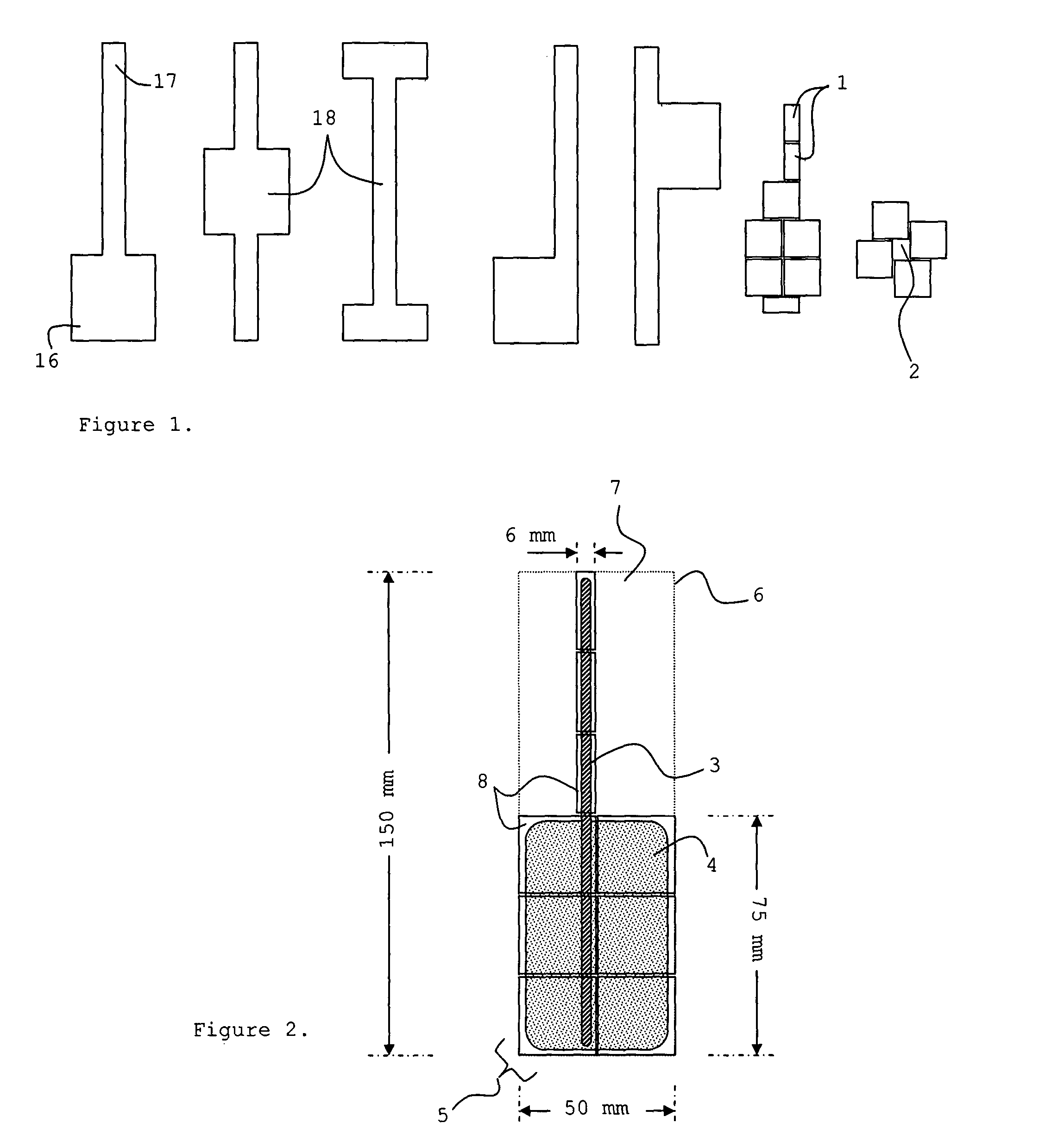
[0026]A preferred shape 5 of the active area of the invented X-ray sensor is shown in FIG. 2. The shape 5 is in this example constructed from nine individual detector elements 8 and is designed for the needs of modern dental extraoral X-ray imaging in which a fan beam 3 is, at the same time, used for panoramic scan imaging and a rectangular cone beam 4 is used for 3D tomographic imaging. Typical dimensions of the preferred active area are given in FIG. 2. As can be observed from FIG. 2,...


PUM


Abstract

A radiation imaging device includes plural individual detectors defining an irregular rectangular active area responsive to x-rays and with different widths along a length of the active area. The individual detectors may be of different rectangular shapes and mounted on a motherboard. The motherboard may be formed of a first module mounting a first of two individual detectors and a second module detachable connected to the first module and mounting a second of two individual detectors.

Description

CROSS REFERENCE TO RELATED APPLICATIONS[0001]The present application claims the benefit of prior filed U.S. patent application Ser. No. 11 / 673,583 filed 11 Feb. 2007 which claimed the benefit of prior filed U.S. patent application Ser. No. 11 / 277,530 filed 27 Mar. 2006, which claimed the benefit of prior filed U.S. Provisional Application Ser. No. 60 / 677,020 filed 2 May 2005, which are all incorporated herein by reference, and to which the present application is a continuation-in-part US national non-provisional utility patent application.BACKGROUND OF THE INVENTION[0002]1. Field of the Invention[0003]The present invention relates to digital radiation imaging. In particular, the invention relates to the effective construction of optimized imaging areas of various size and shape by combining separate semiconductor pixel detectors side by side in a mosaic like manner so that the shape of the active area of the sensor is made to match as exactly as possible the X-ray beam shape (or sha...

Claims


Application Information

Patent Timeline
Patent Type & Authority Patents(United States)
IPC IPC(8): A61B6/14H01L27/146
CPCA61B6/14A61B6/466G01T1/2928G01T1/2018A61B6/547A61B6/12
Inventor SPARTIOTIS, KONSTANTINOSSCHULMAN, TOMPANTSAR, TUOMAS
Owner OY AJAT LTD
Why Eureka
Try Eureka